- News
10 February 2017
New York Power Electronics Manufacturing Consortium produces its first SiC-based patterned wafers
The New York Power Electronics Manufacturing Consortium (NY-PEMC) at SUNY Polytechnic Institute's Albany NanoTech Complex has produced its first silicon carbide (SiC)-based patterned wafer, using SUNY Poly's 150mm SiC processing line (which is claimed to be the first in the USA dedicated to the SiC wafer platform).
"The New York Power Electronics Manufacturing Consortium, led by SUNY Poly, in partnership with New York State and with founding member General Electric, is fast approaching production strength for power electronics," says SUNY Poly's interim president Dr Bahgat Sammakia. "We look forward to continuing to collaborate with GE, New York State, and Empire State Development as SUNY Poly provides SiC wafer production capabilities at its Albany campus, and complementary packaging at its Utica campus, supporting a unique synergy for high-tech research, development, and deployment," he adds.
"This is a significant milestone that brings the NY-PEMC another step closer to full production," notes Empire State Development president, CEO & commissioner Howard Zemsky. "By tapping into the state's skilled workforce and our world-class research and development centers, this public-private partnership will further solidify Upstate New York as the epicenter of developing and producing next-generation chip technologies," he adds.

Picture: The 150mm SiC fab at NY-PEMC.
"As the SiC-based wafer production line continues to advance its capabilities, including reaching this production milestone, General Electric values our strong partnership with SUNY Polytechnic Institute and New York State," comments Danielle Merfeld, vice president & Niskayuna site leader at GE Global Research. "Through the Power Electronics Manufacturing Consortium, we have an opportunity to place the Capital Region, Utica and Upstate New York at the center of the next revolution in power efficiency for electrical machines and systems of all kinds."
The accomplishment is the first step in the qualification of metal-oxide semiconductor field-effect transistor (MOSFET) production for power electronics applications by SUNY Poly's SiC processing line. SiC-based chips provide next-generation capabilities by enabling power devices to get smaller, faster and more efficient as incumbent silicon reaches its physical limits. In particular, SiC-based power electronic devices have the capacity to handle much higher frequencies and temperatures than Si-based devices, which reduces the size and cost of filtering and cooling systems that often must be included as part of an overall system. Additionally, SiC devices can be half the size of similar silicon devices, providing increased power density and reliability. With the improved qualities, SiC-based power devices can enhance a wide range of applications, including in the automotive, clean energy and aeronautics industries, for example.
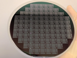
 Picture: NY-PEMC's first patterned SiC wafer.
"The first lot start and first patterned wafer are two goals that have now been achieved, signifying a powerful first step for the PEMC and its production of SiC-based wafers," says Dr Jeffrey Hedrick, principal investigator for NY-PEMC & vice president of SUNY Poly. "We look forward to even more technological achievements as the NY-PEMC further develops the leading-edge SiC-focused capabilities."
SUNY Poly and GE lead the consortium with the goal of developing and producing low-cost, high-performance 6" SiC wafers. The NY-PEMC is a public-private partnership announced in mid-2014. SUNY Poly's 150mm SiC fab is located at its Albany NanoTech Complex, with production coordinated with SUNY Poly's Computer Chip Commercialization Center (Quad-C) at its Utica campus, where the SiC-based power chips will be packaged.
GE and SUNY Poly developing SiC power electronics packaging facility at QUAD C
GE to lead $500m five-year State-funded New York Power Electronics Manufacturing Consortium


