| Home | About Us | Contact Us | Contribute | Advertising | Subscribe for Free NOW! |
| News Archive | Features | Events | Recruitment | Directory |
Contact Details:
k-Space Associates, Inc.
Tel: +1 (734) 426-7977
Fax: +1 (734) 426-7955
Company Profile: k-Space Associates Inc
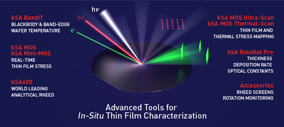
k-Space Associates, Inc. specializes in in-situ, real-time thin-film process monitoring tools for MBE, MOCVD, PVD, and Thermal Evaporation. Applications and materials include the research and production line monitoring of compound semiconductor-based electronic, optoelectronic, and photovoltaic devices. Since 1992 we have been developing quality integrated systems engineered to customers’ input and feedback. Our suite of monitoring tools includes the following:
kSA BandiT wafer temperature monitor: The BandiT systems utilizes diffusely reflected broad band light to accurately and precisely determine wafer temperature. Standard semiconductor substrate materials include GaAs, GaN, ZnO, InP, Si, CIGS, CdTe, Ge, GaSb, GaP, and SiC. BandiT can also spatially resolve temperature across wafers during substrate and multi-wafer platen rotation, yielding true surface temperature maps. Newly developed and patent pending, BlackBody emission monitoring also provides real-time, high resolution temperature monitoring of metal and low E g substrates and films while new spectral analysis routines determine film thickness, growth rate, optical absorption edge, and surface roughness. Unmatched technology and integration options allow for temperature monitoring with better than 1°C accuracy and repeatability with most compound semiconductor materials from RT-1500°C.
kSA MOS thin-film curvature and stress monitor: The patented kSA MOS system utilizes a laser array to determine real-time, 2D thin-film curvature and stress profiles of deposited material or during thermal cycling processes at sample rotation speeds up to 1500rpm. Real-time reflectivity analysis provides important information on thickness, growth rate, and optical constants (n,k). Integration onto most any deposition process chamber is possible with as little as 2mm optical access. Celebrating its 10-year anniversary, kSA MOS is today’s highest performance in-situ curvature/stress system available and is used in leading R&D and production facilities worldwide.
kSA MOS Ultra Scan and kSA Thermal Scan curvature and stress mapping systems: These fully integrated tools map the curvature, stress, and bow height of semiconductor wafers, optical mirrors, lenses, or practically any polished surface. The standard system provides up to 300mm x,y scanning range with 1µm resolution and provides quantitative film stress with full area map. Our Thermal Scan option integrates a fully contained thermal processing chamber for thermal stress analysis up to 1200 °C. kSA MOS-based technology guarantees resolution and repeatability 10X better than any other curvature based method available.
kSA RateRat deposition monitor: The RateRat system uses a powerful "virtual interface" model to fit to reflectivity oscillations in real-time, extracting deposition rates and optical constants (n, k) to very high accuracy. The RateRat system may be used for full process control on MBE, MOCVD, PVD, and other deposition systems.
kSA 400 analytical RHEED system: The kSA 400 is the world's premier analytical RHEED system. Built on 17 years of continuous development, the kSA 400 system offers everything from simple diffraction pattern archiving to complex RHEED analysis. It features three independent methods for deposition rate determination, as well as real-time lattice spacing and surface coherence evolution.
![]() ©2009 Juno Publishing and Media Solutions Ltd. All rights reserved. Semiconductor Today and the editorial material contained within it and related media is the copyright of Juno Publishing and Media Solutions Ltd. Reproduction in whole or part without permission from Juno Publishing and Media Solutions Ltd is forbidden. In most cases, permission will be granted, if the author, magazine and publisher are acknowledged.
©2009 Juno Publishing and Media Solutions Ltd. All rights reserved. Semiconductor Today and the editorial material contained within it and related media is the copyright of Juno Publishing and Media Solutions Ltd. Reproduction in whole or part without permission from Juno Publishing and Media Solutions Ltd is forbidden. In most cases, permission will be granted, if the author, magazine and publisher are acknowledged.
Disclaimer: Material published within Semiconductor Today and related media does not necessarily reflect the views of the publisher or staff. Juno Publishing and Media Solutions Ltd and its staff accept no responsibility for opinions expressed, editorial errors and damage/injury to property or persons as a result of material published.
Semiconductor Today, Juno Publishing and Media Solutions Ltd, Suite no. 133, 20 Winchcombe Street, Cheltenham, GL52 2LY, UK
Web site by No Name No Slogan ![]()