
- Company profile
- EV Group (EVG)
About EV Group (EVG)
EV Group (EVG) is a world leader in wafer-processing solutions for semiconductor, MEMS and nanotechnology applications. Through close collaboration with its global customers, the company implements its flexible manufacturing model to develop reliable, high-quality, low-cost-of-ownership systems that are easily integrated into customers’ fab lines. Key products include wafer bonding, lithography/nanoimprint lithography (NIL) and metrology equipment, as well as photoresist coaters, cleaners and inspection systems.
In addition to its dominant share of the market for wafer bonders, EVG holds a leading position in NIL and lithography for advanced packaging and MEMS. Along these lines, the company co-founded the EMC-3D consortium in 2006 to create and help drive implementation of a cost-effective through-silicon-via (TSV) process for chip packaging and MEMS/sensors. Other target semiconductor-related markets include silicon-on-insulator (SOI), compound semiconductor and silicon-based power-device solutions.
Founded in 1980, EVG is headquartered in St. Florian, Austria, and operates via a global customer support network, with subsidiaries in Tempe, AZ.; Albany, NY; Yokohama and Fukuoka, Japan; Seoul, Korea and Chung-Li, Taiwan. The company's unique Triple i-approach (Invent - Innovate - Implement) is supported by a vertical integration, allowing EVG to respond quickly to new technology developments, apply the technology to manufacturing challenges and expedite device manufacturing in high volume. More information is available at www.EVGroup.com.

EVG Wafer Processing Equipment
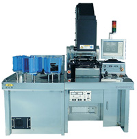
 Automated Mask Alignment System optimized for contactless proximity processing at highest throughput.
The IQ Aligner Automated Mask Alignment System is based on a field-proven, robust design with up to 300 mm wafer size capability, full-field exposure, single and double-side alignment, large gap and dark field mask alignment. The high automation level makes the IQ Aligner Automated Mask Alignment System suitable for volume production applications while tremendously lowering equipment operation and maintenance costs.
Features:
- Manual or fully automated, high-throughput operation
- Full-field exposure, large gap and dark field mask alignment for wafer bumping, chip scale packaging and similar demands
- NanoAlign® featuring high resolution top and bottom side split field microscopes
- Handling of multiple wafer sizes up to 300 mm with quick change-over time
- Windows® based user interface
- Darkfield mask alignment
- Options include automated mask handling and bond alignment capability
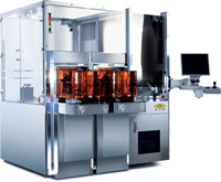
 Fully Automated Wafer Bonding System for HB-LED manufacturing, configurable for all wafer bonding processes eutectic, thermo compression, fusion or LowTemp plasma bonding.
The EVG®560HBL Wafer Bonding System is a dedicated, fully automated wafer bonding system for High-Brightness LED (HB-LED) manufacturing. The flexible tool supports metal, adhesive and fusion bonds of various substrate types. Cassette-to-cassette operation, multi-substrate bonding capability and a modular design with up to four swap-in process modules make the EVG®560HBL the perfect solution for high-volume HB-LED manufacturing. EVG’s field proven wafer bonding technology, as well as our unique approach to low temperature metal wafer bonding, results in highest throughput and yields.
Features:
- Dedicated wafer bonding system for HB-LEDs
- Highest throughput up to 160 bonds/hour (2” wafer equivalents)
- Optimized pressure and temperature uniformity for highest yield
- Automatic handling of bowed and warped wafers
- Eutectic, Transient-Liquid-Phase (TLP) and thermo-compression bonding
- Modular system for high-volume manufacturing, allowing easy switch between wafer sizes
- Total solution fpr HB-LEDs: EVG’s field proven wafer bonding technology with worldwide process engineering support and customer support structure
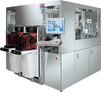 Automated Temporary Bonding / Debonding System for temporary bonding of a substrate on a rigid carrier and debonding, cleaning and unloading of thin wafers.
Increased demand for applications based on thin wafers and microelectronic substrates result in the need for ultra-thin substrate handling and processing. EV Group’s customers benefit from our comprehensive temporary wafer bonding and debonding know-how. On our EVG850TB/DB systems, fragile wafers used in the manufacturing of ICs (memory, CMOS, 3D IC / TSV etc.), power devices, compound semiconductors (e.g. HB-LEDs) and other emerging technologies are temporarily mounted onto solid glass or Silicon carrier wafers for subsequent processing.
Features:
- Bubble-free bonding in a controlled atmosphere
- Wide temperature range for low- and high- temperature adhesives and tapes
- Various carriers (silicon, glass, sapphire, etc…)
- Bridge tool capability
- Automated debonding for thermal release bonding agents such as wax or thermal release dry adhesive
- UV-exposure for debonding of UV-activated tapes
- Automated cleaning of debonded wafer and carrier
- Immediate carrier wafer reuse
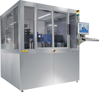
 Automated Mask Alignment System designed for optical double-side lithography. Available in volume production and manual R&D system configurations.
The EVG®6200NT Automated Mask Alignment System offers state-of-the-art features to meet the highest precision and throughput requirements. Based on EVG's flexible and versatile aligner platforms, the system enables manufacturers to easily scale between R&D to volume manufacturing in a simple one-to-one process transfer from manual mode to full automation. The highly advanced “NT Series” system achieves alignment accuracies down to 0.1µm with insitu alignment verification.
Features:
- High resolution top and bottom side split field microscopes
- Handling of multiple wafer sizes with quick change-over
- High degree of automation (multiple send/receive cassettes)
- Manual substrate loading capability on automated system
- Windows® based user interface
- NanoAlign® option for enhanced process capabilities
- Bond alignment option
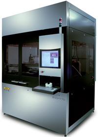 Automated NIL Stepper for Step & Repeat large area UV-Nanoimprinting processes (UV-NIL).
EV Group's EVG770 Automated NIL Stepper is designed for step and repeat large area UV-Nanoimprint Lithography (UV-NIL) processes on 100 - 300 mm wafers, covering applications like life science, optical components, mastering, 3D-Lithography and R&D for semiconductor devices.
Features:
- Vacuum imprinting on a spun-on polymer layer to eliminate defects caused by trapped air bubbles
- Optical sensors for contact-free wedge compensation / non-contact chuck bearing
- High-precision alignment system with accuracy within ± 500 nm (± 50 nm optional)
- Load-cell measurement of embossing/de-embossing force, allowing for real-time, in-situ characterization of resists and anti-sticking layers
- Flexible equipment automation levels for easy and economical transition from R&D to production
- De facto template form factor to shorten the fabrication turnaround time
- Capability to support a host of commercially available resists, improving process flexibility for micro molding and nanopatterning
Contact:
Clemens Schütte
Director Marketing and Communications
EV Group (EVG)
DI Erich Thallner Straße 1
A-4782 St.Florian/Inn
Austria
Phone: + 43 7712 5311 0
E-Mail: C.Schuette@EVGroup.com