| Home | About Us | Contribute | Bookstore | Advertising | Subscribe for Free NOW! |
| News Archive | Features | Events | Recruitment | Directory |
| FREE subscription |
| Subscribe for free to receive each issue of Semiconductor Today magazine and weekly news brief. |
News
21 April 2008
Palomar triples cleanroom capacity for assembly & test services
Palomar Technologies of Carlsbad, CA, USA has tripled cleanroom space for its Palomar Microelectronics assembly & test division and increased its prototyping, applications engineering, process development, volume assembly, and test services capabilities.
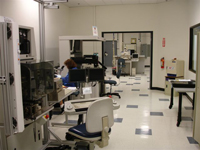 The firm says that its new 2500 square foot (232.26m²) class 100,000 and 500 square foot (46.45m²) class 10,000 cleanrooms enable rapid prototyping and fast turn-around so OEMs can get their products into development or to market faster.
Processes include wire bonding, gold ball bumping, and precision component placement for semiconductor packages, high-power LEDs, MEMS devices, microwave and RF components, optoelectronic packages, multichip modules, and hybrids.
“The new cleanroom space allows us to provide microelectronic services for many of the emerging technologies in areas such as MEMS, high-brightness LEDs, and other advanced packaging applications and to speed delivery of these services,” says Palomar Microelectronics’ operations manager Donald Beck.
Visit: www.palomartechnologies.com
![]() ©2008 Juno Publishing and Media Solutions Ltd. All rights reserved. Semiconductor Today and the editorial material contained within it and related media is the copyright of Juno Publishing and Media Solutions Ltd. Reproduction in whole or part without permission from Juno Publishing and Media Solutions Ltd is forbidden. In most cases, permission will be granted, if the author, magazine and publisher are acknowledged.
©2008 Juno Publishing and Media Solutions Ltd. All rights reserved. Semiconductor Today and the editorial material contained within it and related media is the copyright of Juno Publishing and Media Solutions Ltd. Reproduction in whole or part without permission from Juno Publishing and Media Solutions Ltd is forbidden. In most cases, permission will be granted, if the author, magazine and publisher are acknowledged.
Disclaimer: Material published within Semiconductor Today and related media does not necessarily reflect the views of the publisher or staff. Juno Publishing and Media Solutions Ltd and its staff accept no responsibility for opinions expressed, editorial errors and damage/injury to property or persons as a result of material published.
Semiconductor Today, Juno Publishing and Media Solutions Ltd, Suite no. 133, 20 Winchcombe Street, Cheltenham, GL52 2LY, UK
Web site by No Name No Slogan ![]()