| Home | About Us | Contribute | Bookstore | Advertising | Subscribe for Free NOW! |
| News Archive | Features | Events | Recruitment | Directory |
| FREE subscription |
| Subscribe for free to receive each issue of Semiconductor Today magazine and weekly news brief. |
News
2 December 2008
Controlling crystal structure in nanowire superlattices
Researchers led by professor Lars Samuelson at Lund University’s Nanometer Structure Consortium in Sweden have developed techniques to control the crystal structure of indium arsenide (InAs) nanowires [Caroff et al, Nature Nanotechnology, http://dx.doi.org, published online 30 November 2008].
 Nanowires made of binary semiconductors, such as InAs, often have a high density of twin defects and stacking faults as they grow. This results in a series of different uncontrollable crystal structures, called polytypes.
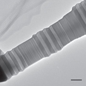
Graphic: TEM image of top of WZ–ZB superlattice nanowire. The gold seed particle is visible at the bottom-left corner. The wider regions are ZB.
The most common polytypes for InAs nanowires are wurtzite (WZ) and zinc-blende (ZB). These effects alter optical and charge-carrier transport properties. The results can be negative, such as scattering from the fault boundaries increasing resistance to current flow. However, such effects, if controllable, could lead to new structures and devices based on band-gap engineering. The energy band offset between the WZ and ZB structures is several tens of milli-electronVolts (meV). In fact, one result of the new WZ-ZB nanowire structures could be a more accurate determination of this offset.
Control over the structure is achieved by varying the size of the gold seed particle and the growth temperature. Smaller-diameter nanowires are largely WZ, moving over to ZB as the diameter increases. Nanowires with diameters of 24nm grown at 460ºC had the WZ structure with a stacking fault density of 2 to 3 per micron. Under the same growth conditions, 110nm diameter wires were ZB and had less than 1 fault/micron. Growth at 420ºC increases the WZ proportion. This enhances the WZ purity at low to medium diameters and creates a large number of twin-plane faults in the ZB phase at larger diameters.
Superlattices consisting of WZ and ZB segments were grown by alternating the growth temperature between 400ºC and 480ºC. Three ZB segments were separated by WZ. The WZ parts showed some single stacking faults. The researchers believe this is the result of non-optimal growth conditions, in particular the switching sequence between the temperatures.
The main energy difference between the WZ and ZB polytypes derives from the ionic interaction between third nearest neighbors. Materials with bonds showing a more ionic nature such as GaN (ionicity 0.557) tend to crystallize as WZ, while lower ionicity materials such GaSb (0.108/0.246) generally go for the ZB form. Between these extremes come the standard III-V semiconductors such as GaAs, GaP, InAs and InP. The Lund team believes that its methods are applicable to GaAs and InP nanowire growth.
The wires were grown using commercial metal-organic chemical vapor deposition (MOCVD) techniques at a pressure of 10kPa with hydrogen as the carrier gas. The precursors were TMIn and AsH 3. The gold particles were deposited on the InAs substrate using a dedicated aerosol system.
Semiconductor nanowires constitute a growing field of research, particularly as the size of commercial devices decrease. In addition to research aimed at characterizing interconnection wires with nano-scale dimensions, there are hopes of using such electronic structures for transistor channels, single-electron memory, nanoelectrodes, photonics (light/laser production, sensing), energy conversion (battery and photovoltaic). Scientific activities include fundamental electron transport studies and chemical and biological sensing and manipulation.
![]() Search: InAs nanowires InAs substrates MOCVD
Search: InAs nanowires InAs substrates MOCVD
Visit: www.nano.lth.se
The author Mike Cooke is a freelance technology journalist who has worked in the semiconductor and advanced technology sectors since 1997.
![]() ©2008 Juno Publishing and Media Solutions Ltd. All rights reserved. Semiconductor Today and the editorial material contained within it and related media is the copyright of Juno Publishing and Media Solutions Ltd. Reproduction in whole or part without permission from Juno Publishing and Media Solutions Ltd is forbidden. In most cases, permission will be granted, if the author, magazine and publisher are acknowledged.
©2008 Juno Publishing and Media Solutions Ltd. All rights reserved. Semiconductor Today and the editorial material contained within it and related media is the copyright of Juno Publishing and Media Solutions Ltd. Reproduction in whole or part without permission from Juno Publishing and Media Solutions Ltd is forbidden. In most cases, permission will be granted, if the author, magazine and publisher are acknowledged.
Disclaimer: Material published within Semiconductor Today and related media does not necessarily reflect the views of the publisher or staff. Juno Publishing and Media Solutions Ltd and its staff accept no responsibility for opinions expressed, editorial errors and damage/injury to property or persons as a result of material published.
Semiconductor Today, Juno Publishing and Media Solutions Ltd, Suite no. 133, 20 Winchcombe Street, Cheltenham, GL52 2LY, UK
Web site by No Name No Slogan ![]()