| Home | About Us | Contribute | Bookstore | Advertising | Subscribe for Free NOW! |
| News Archive | Features | Events | Recruitment | Directory |
| FREE subscription |
| Subscribe for free to receive each issue of Semiconductor Today magazine and weekly news brief. |
News
11 February 2008
EC project investigating non-Si channels for post-22nm CMOS
Co-funded by a grant of €5.8m from the European Commission as the ‘flagship’ for CMOS R&D in its 7th Framework program (FP7) in Information and Communication Technologies, the €9.1m, 36 month project ‘Dual channel CMOS for (sub)-22nm high performance logic’ (DUALLOGIC) was launched in December by a consortium consisting of: the National Center for Scientific Research (NCSR) DEMOKRITOS in Athens, Greece; research institute IMEC and Katholieke Universiteit Leuven in Belgium; IBM-Zurich in Switzerland; CEA-LETI and chip maker ST Microelectronics-Crolles in France; chip maker NXP Semiconductors of The Netherlands; epitaxial deposition equipment maker Aixtron of Aachen, Germany; and the University of Glasgow, UK.
Led by Dr Athanasios Dimoulas of NCSR DEMOKRITOS, the DUALLOGIC project aims to shape CMOS generations beyond 22nm with innovations in nano-electronic materials, equipment, processing and device integration on silicon.
Late 2007 was marked by what was described by Intel’s Gordon Moore as the “biggest change in transistor technology in 40 years”: the replacement of the polySi/SiO2 gate stack by a metal/high-k dielectric combination in the 45nm generation of CMOS (now in production). To break the performance barrier beyond the 22nm node, the next element of the MOS transistor to be replaced may be the active channel.
Replacing silicon in the channel by germanium (in which charge carriers have higher mobility) can significantly enhance transistor performance but, after five years of intensive research, Ge has been found to only outperform Si for the p-type doped pMOS transistor - not the n-type doped nMOS transistor - in complementary metal-oxide semiconductor (CMOS) ICs. So, CMOS technology made entirely of Ge-channel MOS transistors does not seem to be feasible at present.
In contrast, III-V compound semiconductor materials such as gallium arsenide (GaAs) and indium gallium arsenide (InGaAs) are effective for nMOS but seem to be unsuitable for pMOS. DUALLOGIC therefore targets the co-integration of Ge pMOS and III-V nMOS side-by-side on a complex engineered substrate on silicon to demonstrate dual-channel CMOS technology for the first time.
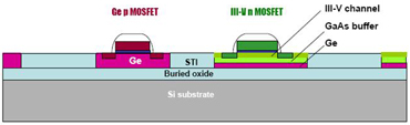
Picture: Cross-sectional structure of dual-channel CMOS logic.
The project’s main objectives are to:
- demonstrate the co-integration of functional high-mobility Ge pMOS and III-V nMOS on the same engineered substrate by using a silicon-compatible process in a 65nm/200mm pilot line, showing that that dual-channel front-end-of-line (FEOL) CMOS technology is scalable and manufacturable;
- investigate short-channel, leakage and transport effects and fundamental materials problems in aggressively scaled high-channel-mobility devices;
- prepare the take-up of project results by the end of 2009 in a broader 22nm or sub-22nm technology platform by integrating dual-channel FEOL technology with back-end and device architecture modules that could be implemented within a future, larger FP7 R&D project.
Development work includes the full set of FEOL modules: 200mm local germanium-on-insulator (GeOI) by Ge condensation (by CEA-LETI and ST); MOCVD equipment and processes for selective epitaxy of III-V compounds on Ge (Aixtron); dual-channel engineered substrates (IMEC); co-integration of short-channel functional transistors using a 65nm/200mm pilot line (IMEC and IBM); development of the gate stack (NCSR- DEMOKRITOS and KU Leuven); and device modelling and circuit design (NXP and the University of Glasgow).
Besides their high mobility, the channel materials being investigated have other interesting properties that make them attractive beyond the context of device scaling for logic, such as in applications where lower supply voltages are needed to combine low power with high performance. DUALLOGIC could hence create a generic material and technology platform that could allow significant diversification in on-chip functionality. It could also be a catalyst for the convergence of 2020 nanoelectronic technologies, as foreseen in the research agenda of Europe’s ENIAC technology platform.
See related items:
InGaAs emerging as material for future NMOS channels
IMEC reports record-performance Ge pMOS FETs using Si-compatible processing
Visit: www.ims.demokritos.gr/DUALLOGIC
![]()
![]() ©2008 Juno Publishing and Media Solutions Ltd. All rights reserved. Semiconductor Today and the editorial material contained within it and related media is the copyright of Juno Publishing and Media Solutions Ltd. Reproduction in whole or part without permission from Juno Publishing and Media Solutions Ltd is forbidden. In most cases, permission will be granted, if the author, magazine and publisher are acknowledged.
©2008 Juno Publishing and Media Solutions Ltd. All rights reserved. Semiconductor Today and the editorial material contained within it and related media is the copyright of Juno Publishing and Media Solutions Ltd. Reproduction in whole or part without permission from Juno Publishing and Media Solutions Ltd is forbidden. In most cases, permission will be granted, if the author, magazine and publisher are acknowledged.
Disclaimer: Material published within Semiconductor Today and related media does not necessarily reflect the views of the publisher or staff. Juno Publishing and Media Solutions Ltd and its staff accept no responsibility for opinions expressed, editorial errors and damage/injury to property or persons as a result of material published.
Semiconductor Today, Juno Publishing and Media Solutions Ltd, Suite no. 133, 20 Winchcombe Street, Cheltenham, GL52 2LY, UK
Web site by No Name No Slogan ![]()