| Home | About Us | Contribute | Bookstore | Advertising | Subscribe for Free NOW! |
| News Archive | Features | Events | Recruitment | Directory |
WAFER PROCESSING
Achieve accurate and repeatable processing results with Logitech's semiconductor equipment.


| FREE subscription |
| Subscribe for free to receive each issue of Semiconductor Today magazine and weekly news brief. |
News
30 May 2008
PbSe research resurrects nanocrystal avalanche hopes
Delft University of Technology and Cornell University researchers have shown that carrier multiplication can occur in photo-absorption in nanocrystals (NCs) [Tuan Trinh et al, Nano Letters, ASAP online publication, May 20, 2008], despite previous adverse reports.
Carrier multiplication (CM), or avalanching, refers to carriers created well away from band minima (see figure) that lose energy by creating extra electron-hole pairs (excitons) rather than by generating heat (phonons). Getting more electrons, rather than heat, out of each photon could boost solar cell efficiencies to 44%, it has been estimated.
Efficient CM had been reported in experiments on a number of nanocrystal systems including lead selenide (PbSe), lead sulfide (PbS), lead telluride (PbTe), cadmium selenide (CdSe), indium arsenide (InAs), and silicon (Si). These studies compared the fast decay of multi-exciton systems resulting from CM with the slow relaxation of single excitons.
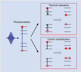
Picture: Schematic of high-energy charge carriers losing energy through thermal
relaxation (top) or carrier multiplication (bottom).
Unfortunately, these results did not stand up under more elaborate scrutiny, where results from CdSe and CdTe NC photoluminescence gave a negligible efficiency for CM production. Some researchers studying InAs NCs withdrew their results and again a closer study (the majority of whose authors were involved in the earlier paper) suggests that there is no detectable CM in this system.
These negative results in specific systems have therefore cast a shadow of doubt over previous results in other materials. The Delft/Cornell research lifts this cloud somewhat by showing that CM can occur in PbSe NCs. However, the efficiency that is measured is lower than previously reported, and there may not be any confinement advantage from using NCs as opposed to bulk material.
The Delft and Cornell researchers used pump-probe transient absorption (TA) measurements on PbSe nanocrystals grown in solution to rule out possible alternative mechanisms that could mimic carrier multiplication (CM). The TA signal measures the femtosecond transient photo-bleaching effect of the pump signal on photo-absorption from the probe beam. The NCs are described as monodisperse and quasi-spherical, with diameters of 6.8nm as determined from the energy of the first exciton absorption line at 0.65eV.
The two main alternatives that can mask CM are multiphoton absorption and charge trapping. Multiphoton absorption is excluded by reducing the pump power to a level where the photon ‘fluence’ is so low that only CM can occur.
The researchers see charge trapping as requiring a number of coincidences to produce a signal that would appear similar to CM. To rule out such a possibility, sub- and super-threshold signals (again at low fluence) were compared at long delay times so that CM effects do not contribute to the signal. The sub-threshold part was carried out at 1.55eV and super-threshold at 3.1eV. The long decay component (100ps due to a single exciton per photon) is the same in both situations, excluding trapping according to the researchers. The fast CM decay signal sits on top of this background.
In addition, the research attempted to get a quantitative measure of CM efficiency. Somewhat disappointingly, the group found no discernable enhancement from the use of nanocrystal confinement effects compared with measurements made on bulk PbSe 50 years ago [Smith and Dutton, J. Opt. Soc. Am., vol.48, p.1007, 1958]. The CM efficiency is also only slightly higher than that observed in Si or Ge.
The leader of the Delft team, professor Laurens Siebbeles, believes that this research paves the way for further unraveling the secrets of the avalanche effect.
Search: Solar cells PbSe InAs CdTe
Visit: http://dx.doi.org/10.1021/nl0807225
The author Mike Cooke is a freelance technology journalist who has worked in the semiconductor and advanced technology sectors since 1997.
![]()
![]() ©2008 Juno Publishing and Media Solutions Ltd. All rights reserved. Semiconductor Today and the editorial material contained within it and related media is the copyright of Juno Publishing and Media Solutions Ltd. Reproduction in whole or part without permission from Juno Publishing and Media Solutions Ltd is forbidden. In most cases, permission will be granted, if the author, magazine and publisher are acknowledged.
©2008 Juno Publishing and Media Solutions Ltd. All rights reserved. Semiconductor Today and the editorial material contained within it and related media is the copyright of Juno Publishing and Media Solutions Ltd. Reproduction in whole or part without permission from Juno Publishing and Media Solutions Ltd is forbidden. In most cases, permission will be granted, if the author, magazine and publisher are acknowledged.
Disclaimer: Material published within Semiconductor Today and related media does not necessarily reflect the views of the publisher or staff. Juno Publishing and Media Solutions Ltd and its staff accept no responsibility for opinions expressed, editorial errors and damage/injury to property or persons as a result of material published.
Semiconductor Today, Juno Publishing and Media Solutions Ltd, Suite no. 133, 20 Winchcombe Street, Cheltenham, GL52 2LY, UK
Web site by No Name No Slogan ![]()