| Home | About Us | Contribute | Bookstore | Advertising | Subscribe for Free NOW! |
| News Archive | Features | Events | Recruitment | Directory |
| FREE subscription |
| Subscribe for free to receive each issue of Semiconductor Today magazine and weekly news brief. |
News
30 September 2008
LayTec to develop in-situ sensor for ISE’s triple-junction PV cells
 LayTec GmbH of Berlin, Germany says that the German Federal Ministry of Economics and Technology (Bundesministerium für Wirtschaft und Technologie) has approved funding within the PRO Inno Program for the development of a new in-situ sensor for the photovoltaic market.
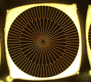
Picture: Multi-junction concentrator solar cell with an efficiency of 39.7% at a concentration factor of 300, developed at Fraunhofer ISE.
In collaboration with the Fraunhofer Institute for Solar Energy Systems (ISE) in Freiburg, Germany, a research project has been launched to improve the in-situ monitoring of MOCVD processes for triple-junction photovoltaic cells being developed at Fraunhofer ISE (which recently set the European record for solar cell efficiency, at 39.7%). Cooperation between LayTec and ISE's III-V Epitaxy and Solar Cells group is aimed at developing monitoring sensors for industrial-scale manufacturing of triple-junction solar cells with improved process control in multi-wafer MOCVD reactors. “Real-time analysis and control of our processes is becoming a key for the development of complex semiconductor structures such as multi-junction solar cells” says Dr Frank Dimroth, head of ISE’s III-V Epitaxy and Solar Cells group.
ISE's cells are the most efficient produced in Europe. ISE transfers its process technology to the cooperation partner Azur Space Solar Power GmbH of Heilbronn, Germany (Azur SSP), which prepares them for commercial production. ISE and Azur SSP use Aixtron Planetary systems for both development and manufacturing. LayTec's EpiCurveTT sensor, which the firm claims is already the bestseller for the MOCVD LED market, will be further improved to achieve the resolution necessary for multi-junction solar cell growth under the conditions of planetary rotation. In addition to temperature, layer thickness and strain measurements, the new sensor aims to determine the composition and help to better understand the reasons for dislocations and strain within the layers. This will help to compensate for strain-induced temperature inhomogeneities, to determine the thickness of individual thin layers and to monitor the composition of critical heterojunctions, says LayTec.
*LayTec has recruited Dr Qi Cao as a sales engineer. After graduating in physics from China's Nanjing University of Science and Technology, Cao undertook research on optical features of nano-structure materials and obtained a PhD in Optical Engineering in 2004, before continuing research on laser transmission characteristics of nano-holes at Germany's Konstanz University and finally focusing on opto-electric features of single molecules at Münster University. Since 2006, she has gained experience in sales and customer support working for Olympus Microscope in the USA.
At LayTec, Cao will be in charge of sales activities mainly in Taiwan and Greater China, and will support customers and distributors worldwide.
See related item:
Fraunhofer ISE raises Euro PV efficiency record to 39.7%
Search: LayTec Fraunhofer In-situ monitoring Triple-junction photovoltaic cells MOCVD
Visit: www.laytec.de
![]()
![]() ©2008 Juno Publishing and Media Solutions Ltd. All rights reserved. Semiconductor Today and the editorial material contained within it and related media is the copyright of Juno Publishing and Media Solutions Ltd. Reproduction in whole or part without permission from Juno Publishing and Media Solutions Ltd is forbidden. In most cases, permission will be granted, if the author, magazine and publisher are acknowledged.
©2008 Juno Publishing and Media Solutions Ltd. All rights reserved. Semiconductor Today and the editorial material contained within it and related media is the copyright of Juno Publishing and Media Solutions Ltd. Reproduction in whole or part without permission from Juno Publishing and Media Solutions Ltd is forbidden. In most cases, permission will be granted, if the author, magazine and publisher are acknowledged.
Disclaimer: Material published within Semiconductor Today and related media does not necessarily reflect the views of the publisher or staff. Juno Publishing and Media Solutions Ltd and its staff accept no responsibility for opinions expressed, editorial errors and damage/injury to property or persons as a result of material published.
Semiconductor Today, Juno Publishing and Media Solutions Ltd, Suite no. 133, 20 Winchcombe Street, Cheltenham, GL52 2LY, UK
Web site by No Name No Slogan ![]()