| Home | About Us | Contribute | Bookstore | Advertising | Subscribe for Free NOW! |
| News Archive | Features | Events | Recruitment | Directory |
| FREE subscription |
| Subscribe for free to receive each issue of Semiconductor Today magazine and weekly news brief. |
News
3 September 2008
Positive result from negative index using InGaAsP
Negative refractive index researchers at Northeastern University (Boston, MA, USA) have moved on from ‘metamaterial’ structures consisting of alumina rods and microwave sources to sub-micron scale InGaAsP semiconductors and infrared light [Casse et al, App. Phys. Lett., vol.93, p.053111, 2008]. Negative refractive index material optical systems have been considered theoretically since 1968, but have only recently been realized in metamaterials.
The negative index has the potential for making more compact lenses with increased numerical aperture, reduced spot size (close to diffraction limit) and reduced spherical aberration using concave surfaces, compared with normal convex lenses.
The Northeastern effective negative refractive index metamaterial consisted of a two-dimensional (2D) square lattice of airholes etched into an InP/InGaAsP heterostructure. The holes had diameters of 295nm, and were placed 470nm apart. The IR light travelled through a 400nm thick InGaAsP waveguide layer sandwiched between cladding layers of InP (200nm top, 300nm bottom) on an InP substrate (Figure 1).
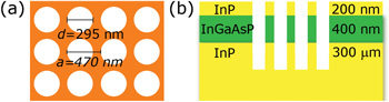
Figure 1. Top and side views of InGaAsP photonic crystal with negative refractive index ~-0.7 at λ ~ 1530nm.
A dispersion/band structure calculation of light travelling through such a ‘photonic crystal’ suggests that for IR light of wavelength (λ) around 1.5 µm the effective refractive index is ~-0.7.
The researchers tested their expectations in a concave lens system produced in the plane of the InGaAsP light conducting layer (Figure 2). The negative refractive index enables a real focus to result from a concave lens; just as a convex surface results in a real focus for the positive index of normal materials. The Northeastern lens had a 20 µm radius for the concave surface and the expected focal length was at 12 µm. The numerical aperture was close to 1.
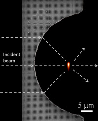 Measurements using a near-field scanning optical microscope (NSOM) gave a full-width at half maximum (FWHM) for the focal spot of 0.68 λ for 1.53 µm (1530nm) wavelength light. This is very close to the diffraction limit (~0.5 λ). A simulation of the system gave an expected FWHM of 0.67 λ. The measured focal length was the expected 12 µm (~8 λ).
Figure 2. Plano-convex lens constructed using the metamaterial/photonic crystal.
Since the materials of the system are purely dielectric, the intrinsic power losses are much lower than those of traditional metamaterial negative refractive systems that contain conducting metal. Extrinsic losses of the InGaAsP system are expected only from imperfections in nanofabrication, and from couplings and interfaces.Search: InGaAsP InP substrate
Visit: www.northeastern.edu
The author Mike Cooke is a freelance technology journalist who has worked in the semiconductor and advanced technology sectors since 1997.
![]()
![]() ©2008 Juno Publishing and Media Solutions Ltd. All rights reserved. Semiconductor Today and the editorial material contained within it and related media is the copyright of Juno Publishing and Media Solutions Ltd. Reproduction in whole or part without permission from Juno Publishing and Media Solutions Ltd is forbidden. In most cases, permission will be granted, if the author, magazine and publisher are acknowledged.
©2008 Juno Publishing and Media Solutions Ltd. All rights reserved. Semiconductor Today and the editorial material contained within it and related media is the copyright of Juno Publishing and Media Solutions Ltd. Reproduction in whole or part without permission from Juno Publishing and Media Solutions Ltd is forbidden. In most cases, permission will be granted, if the author, magazine and publisher are acknowledged.
Disclaimer: Material published within Semiconductor Today and related media does not necessarily reflect the views of the publisher or staff. Juno Publishing and Media Solutions Ltd and its staff accept no responsibility for opinions expressed, editorial errors and damage/injury to property or persons as a result of material published.
Semiconductor Today, Juno Publishing and Media Solutions Ltd, Suite no. 133, 20 Winchcombe Street, Cheltenham, GL52 2LY, UK
Web site by No Name No Slogan ![]()