| Home | About Us | Contribute | Bookstore | Advertising | Subscribe for Free NOW! |
| News Archive | Features | Events | Recruitment | Directory |
| FREE subscription |
| Subscribe for free to receive each issue of Semiconductor Today magazine and weekly news brief. |
News
15 April 2009
First all-optical silicon-based signal processing for transmission above 100Gb/s
A collaboration between the University of Karlsruhe, Germany, IMEC in Leuven, Belgium, Lehigh University in the USA, and ETH Zürich in Switzerland has resulted in the first experimental proof of all-optical ultra-fast communication signal processing with silicon-based devices for transmission speeds above 100Gb/s (C. Koos et al, Nature Photonics, April 2009, vol 3, issue 4, p216). The achievement is claimed as a key step towards the development of complex silicon-based photonic integrated circuits (PICs).
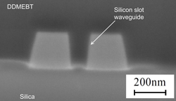 Picture:
Scanning electron microscope image of the cross-section of the vapor-deposited organic film covering the silicon waveguide, which is patterned on a silicon-on-insulator substrate.
Picture:
Scanning electron microscope image of the cross-section of the vapor-deposited organic film covering the silicon waveguide, which is patterned on a silicon-on-insulator substrate.
All-optical signal processing is of particular interest for telecoms applications, where speed, power and cost are crucial. A key element is an optical waveguide with highly nonlinear and ultra-fast performance. Researchers from the University of Karlsruhe, IMEC (and its associated laboratory INTEC at Ghent University), Lehigh University, and ETH Zürich fabricated an optical waveguide structure by combining deep-ultraviolet lithography, standard CMOS processing and organic molecular beam deposition. This 'silicon-organic hybrid' (SOH) approach enables the fabrication of waveguides that pave the way towards all-optical processing.
A 4mm long SOH waveguide with a record nonlinearity coefficient of about 105(Wkm)-1 in the 1.55µm telecom window proved the capability of the SOH concept. Record values predicted by theory have hence been confirmed experimentally for the first time. Based on these waveguides, all-optical demultiplexing of a 170.8Gb/s telecom signal to 42.7Gb/s was performed using four-wave mixing. This is claimed to be the fastest silicon photonic optical signal processing demonstrated to date. This experiment hence proved the viability of the SOH waveguides for all-optical processing of broadband telecom signals.
With the SOH approach, some inherent limitations of silicon could be overcome, say the researchers. Silicon-based technology, in particular silicon-on-insulator (SOI) technology, has already proven very successful for the fabrication of various passive linear optical devices such as filters. The development of ultra-fast active Si-based functionalities, such as all-optical switching, remained challenging due to the slow dynamics caused by unwanted non-linear effects in silicon. So far, the data rate achieved by using bare silicon waveguides was limited to only 40Gb/s.
The SOH approach overcomes this intrinsic limitation - thus enabling data rates above 100Gb/s - by combining the best of two worlds: mature CMOS processing is used to fabricate the waveguide, and organic molecular beam deposition is used to cover it with organic molecules.
These molecules efficiently transfer all-optical interaction without introducing significant absorption. The ability of the organic material to homogeneously fill the slot between the waveguides is a key feature of the deposition process.
The silicon circuits were designed by researchers at the University of Karlsruhe in a fabless way, and were fabricated through the ePIXfab service on IMEC's 200mm silicon photonics platform. ePIXfab is a European-funded initiative coordinated by IMEC to
allow cost-effective fabless prototyping in wafer-scale silicon photonics technology for R&D. The service runs multi-project wafer shuttles in which designs from users worldwide share mask and processing costs.
![]() Search: IMEC Lehigh University ETH Silicon PICs
Search: IMEC Lehigh University ETH Silicon PICs
Visit: www.nature.com

![]() ©2009 Juno Publishing and Media Solutions Ltd. All rights reserved. Semiconductor Today and the editorial material contained within it and related media is the copyright of Juno Publishing and Media Solutions Ltd. Reproduction in whole or part without permission from Juno Publishing and Media Solutions Ltd is forbidden. In most cases, permission will be granted, if the author, magazine and publisher are acknowledged.
©2009 Juno Publishing and Media Solutions Ltd. All rights reserved. Semiconductor Today and the editorial material contained within it and related media is the copyright of Juno Publishing and Media Solutions Ltd. Reproduction in whole or part without permission from Juno Publishing and Media Solutions Ltd is forbidden. In most cases, permission will be granted, if the author, magazine and publisher are acknowledged.
Disclaimer: Material published within Semiconductor Today and related media does not necessarily reflect the views of the publisher or staff. Juno Publishing and Media Solutions Ltd and its staff accept no responsibility for opinions expressed, editorial errors and damage/injury to property or persons as a result of material published.
Semiconductor Today, Juno Publishing and Media Solutions Ltd, Suite no. 133, 20 Winchcombe Street, Cheltenham, GL52 2LY, UK
Web site by No Name No Slogan ![]()