| Home | About Us | Contribute | Bookstore | Advertising | Subscribe for Free NOW! |
| News Archive | Features | Events | Recruitment | Directory |
| FREE subscription |
| Subscribe for free to receive each issue of Semiconductor Today magazine and weekly news brief. |
News
28 April 2009
Braunschweig buys LayTec EpiCurve TT for long-wavelength GaN R&D
LayTec GmbH of Berlin, Germany, which provides in-situ thin-film monitoring systems, says that it has sold an EpiCurve TT system to the Technical University of Braunschweig, Germany.
The tool will be used by the group of professor A. Hangleiter for R&D on gallium nitride-based long-wavelength emitters (mainly green lasers and LEDs).
Specifically, Dr Uwe Rossow will use the EpiCurve TT to monitor and understand the strain effects and the relaxation process of the underlying cladding and waveguide layers as well as of the layers in the active region of the emitting structures. His team uses indium gallium nitride (InGaN) in the quantum wells.
The EpiCurve TT measures in-situ wafer bowing, temperature and reflectance, which helps to control stress, film composition, surface roughness and wafer temperature.
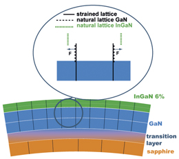 Figure 1 shows roughly what happens when strained InGaN is grown on a GaN buffer: a layer of InGaN, which has a lattice constant that is larger than the underlying layer, forces the whole stack to bow. The wafer becomes convex, which causes temperature deviations in the middle and on the edges of the structure.
Figure 1: Model of the wafer bow process due to increasing indium content: composition-induced lattice mismatch causes wafer bow and temperature deviations.
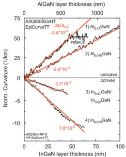 Figure 2 shows an example of curvature measurements during the growth of ternary InGaN and AlGaN layers. Both the film composition and strain-induced relaxation can be detected.
Figure 2: Curvature measurements of ternary layer growth: compressive stress (InGaN) causes convex bow; tensile strain (AlGaN) causes concave bow.
“Simultaneous curvature and temperature measurements by EpiCurve TT already during the process will help us to control the relaxation process, to achieve better uniformity, to reproduce growth conditions and improve the structure quality,” comments Rossow.
LayTec to hold first user meetings in Taiwan
Since its market share in Taiwan is growing rapidly, LayTec says that, in cooperation with Taiwan distributor and service partner Challentech International Corp, it is organizing two user meetings for customers in Taiwan: one in Hsinchu on 23 June and another in Tainan on 25 June.
At the meetings, LayTec's engineers and customers will present measurement results and share their experience and data analysis for MOCVD process evaluation. In addition, LayTec will report on the latest developments, answer users' questions, and give practical advice.
Customers in Taiwan will receive a personal invitation from Taiwan Challentech International Corp by the end of April.
11th in-situ seminar for customers
In conjunction with the 13th European Workshop on Metalorganic Vapor Phase Epitaxy (EWMOVPE XIII)in Ulm, Germany, Laytec is organizing its 11th in-situ seminar for customers in the Edwin-Schaff Congress Center on 7 June.
See related items:
LayTec sells 100th EpiCurveTT sensor; recruits new sales engineer
LayTec wafer curvature sensors sold for European R&D
![]() Search: LayTec In-situ monitoring MOVPE MOCVD
Search: LayTec In-situ monitoring MOVPE MOCVD
Visit: www.laytec.de

![]() ©2009 Juno Publishing and Media Solutions Ltd. All rights reserved. Semiconductor Today and the editorial material contained within it and related media is the copyright of Juno Publishing and Media Solutions Ltd. Reproduction in whole or part without permission from Juno Publishing and Media Solutions Ltd is forbidden. In most cases, permission will be granted, if the author, magazine and publisher are acknowledged.
©2009 Juno Publishing and Media Solutions Ltd. All rights reserved. Semiconductor Today and the editorial material contained within it and related media is the copyright of Juno Publishing and Media Solutions Ltd. Reproduction in whole or part without permission from Juno Publishing and Media Solutions Ltd is forbidden. In most cases, permission will be granted, if the author, magazine and publisher are acknowledged.
Disclaimer: Material published within Semiconductor Today and related media does not necessarily reflect the views of the publisher or staff. Juno Publishing and Media Solutions Ltd and its staff accept no responsibility for opinions expressed, editorial errors and damage/injury to property or persons as a result of material published.
Semiconductor Today, Juno Publishing and Media Solutions Ltd, Suite no. 133, 20 Winchcombe Street, Cheltenham, GL52 2LY, UK
Web site by No Name No Slogan ![]()