| Home | About Us | Contribute | Bookstore | Advertising | Subscribe for Free NOW! |
| News Archive | Features | Events | Recruitment | Directory |
| FREE subscription |
| Subscribe for free to receive each issue of Semiconductor Today magazine and weekly news brief. |
News
14 April 2009
sp3 launches 2-4” silicon-on-diamond wafers for high-power, high-frequency devices
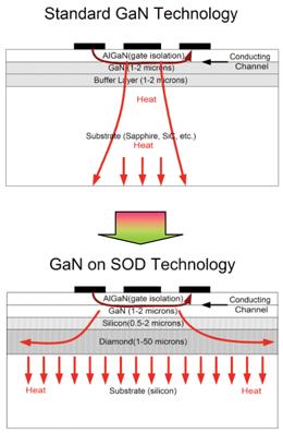
sp3 Diamond Technologies Inc of Santa Clara, CA, USA is taking orders for 2-inch and 4-inch silicon on diamond (SOD) wafers for use as gallium nitride (GaN) substrates and accelerating development of 6-inch wafers for use as laterally diffused metal oxide semiconductor (LDMOS) substrates.
sp3 claims that, because of improved thermal conductivity over traditional silicon wafers, its SOD wafers deliver higher thermal conductivity at a lower cost than existing silicon carbide (SiC) alternatives for GaN and for higher-performance LDMOS devices.
SOD wafers deliver a high-performance path for devices designed for WiMax base-stations and other commercial and military broadband and high-power switching applications (including radar communications equipment, weather and communications satellite equipment and hybrid power switching devices). sp3 says that its new product offering seeks to address the current performance limitations of these devices, as they become increasingly impacted by the thermal restrictions of silicon wafers or the extreme cost and lower performance of SiC wafers.
 “High-power, high-frequency devices – such as high-power radar and RF amplifiers, and DC-to-DC and AC-to-DC converters – have performance limitations due to the physical structure of standard silicon substrates,” says president & chief operating officer Dwain Aidala. “Military and industrial applications stand to benefit significantly from building devices on a diamond substrate with a device-quality, thin silicon top layer,” he adds. “GaN or LDMOS devices built on such a structured substrate can be driven to significantly higher power levels than current alternatives, thereby maximizing performance.” The SOD wafers are available at a lower cost than alternative diamond-based solutions or traditional SiC substrates, the firm claims.
The wafers are delivered as structured substrates with a top layer of device-quality float-zone silicon. They provide diamond heat spreading directly under the junction and can achieve more than a 100% increase in power levels compared to silicon substrates alone, and a 50-80% increase compared to SiC, at a fixed junction temperature, it is claimed. At fixed power, they can reduce junction temperature by more than 50 degrees compared to GaN on silicon or SiC. GaN growth on SOD yields epitaxial films equivalent to GaN on silicon, and wafer size can be scaled up to 300mm, sp3 adds.
2-inch and 4-inch SOD wafers with a silicon top layer are currently available for GaN devices, as well as with a GaN epitaxial layer (GaN on SOD wafers) for manufacturers without an in-house epitaxial deposition capability.
![]() Search: sp3 Diamond Technologies GaN substrates LDMOS SiC wafers
Search: sp3 Diamond Technologies GaN substrates LDMOS SiC wafers
Visit: www.sp3diamondtech.com

![]() ©2009 Juno Publishing and Media Solutions Ltd. All rights reserved. Semiconductor Today and the editorial material contained within it and related media is the copyright of Juno Publishing and Media Solutions Ltd. Reproduction in whole or part without permission from Juno Publishing and Media Solutions Ltd is forbidden. In most cases, permission will be granted, if the author, magazine and publisher are acknowledged.
©2009 Juno Publishing and Media Solutions Ltd. All rights reserved. Semiconductor Today and the editorial material contained within it and related media is the copyright of Juno Publishing and Media Solutions Ltd. Reproduction in whole or part without permission from Juno Publishing and Media Solutions Ltd is forbidden. In most cases, permission will be granted, if the author, magazine and publisher are acknowledged.
Disclaimer: Material published within Semiconductor Today and related media does not necessarily reflect the views of the publisher or staff. Juno Publishing and Media Solutions Ltd and its staff accept no responsibility for opinions expressed, editorial errors and damage/injury to property or persons as a result of material published.
Semiconductor Today, Juno Publishing and Media Solutions Ltd, Suite no. 133, 20 Winchcombe Street, Cheltenham, GL52 2LY, UK
Web site by No Name No Slogan ![]()