| Home | About Us | Contribute | Bookstore | Advertising | Subscribe for Free NOW! |
| News Archive | Features | Events | Recruitment | Directory |
| FREE subscription |
| Subscribe for free to receive each issue of Semiconductor Today magazine and weekly news brief. |
News
8 December 2009
Long-term thermal probe into GaN-Schottky performance
European researchers have built Schottky diodes on free-standing gallium nitride (FS-GaN) substrates that can withstand storage temperatures up to 400°C [O’Mahony et al, Semicond. Sci. Technol., vol24, p125008, 2009]. Such devices have been of interest lately with a view to application in hybrid electric vehicles and other high-temperature environments (e.g. aerospace equipment). This would add a further capability for the commercial deployment of GaN in addition to visible–ultaviolet light emission and use in radio/microwave power amplification.
GaN has a wide bandgap (~3.5eV) that leads to a high breakdown field (~2-3x10⁶V/cm) and high thermal conductivity (1W/cm-K). In theory, GaN-based Schottky devices should exhibit lower values for intrinsic leakage and specific on-resistance. Further, the ability to operate at higher temperatures than present-day silicon-based devices (~150°C) would reduce/simplify or even remove the need for associated cooling equipment.
As usual in such work, there are barriers to achieving optimum performance. In nitride-based devices, substrate material quality is a particular concern, since GaN is difficult to grow with low threading dislocation defect levels. For the high-temperature Schottky diode application, it is also important to find a thermally stable metal combination for the Schottky contact with the GaN material.
Free-standing GaN substrates are often used to reduce defect levels in subsequent epitaxial layers, compared with GaN grown epitaxially on sapphire or silicon. In addition, the substrate can be made electrically conductive with n-type silicon doping, allowing a vertical rather than planar structure to be realized for better power and thermal characteristics (less current crowding, better heat dissipation and better reverse breakdown).
 Nickel is a popular Schottky metal for GaN. However, at high temperature (greater than 500°C) problems arise, such as Ga and N out-diffusion, and intermixing to form Ni-Ga or metal nitrides.
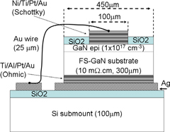
Figure: Schematic of packaged GaN-Schottky diode.
The researchers — based in Ireland (Tyndall National Institute), Germany (AZUR Space GmbH), Netherlands (European Space Agency) and UK (Imperial College) — used 50mm-diameter FS-GaN substrates from Lumilog. The FS-GaN substrates are grown using hydride vapor phase epitaxy (HVPE) to create a 300μm-thick layer of GaN on sapphire that is then separated from the sapphire. The researchers grew a lightly doped n-GaN epitaxial layer on the FS-GaN using metal-organic chemical vapor deposition (MOCVD). The ohmic contact (Ti/Al/Pt/ Au; 3/50/50/ 200nm) was deposited on the unpolished back-side of the substrate.
The Schottky top contact was designed using a nitride over gallide (NOG) technique developed at the University of Florida. In NOG, nickel is thought to form a stable gallide interface with the GaN and titanium forms a nitride to prevent nitrogen out-diffusion. The contact used in the European work consisted of (Ni/Ti/Pt/Au; 50/10/50/ 200nm) evaporated into a 100μm-diameter hole formed in a 200nm silicon dioxide layer.
The resulting diodes had a low forward voltage (less than 1.5V) and low on-resistance (0.3mΩcm2) at high current density (1300A/cm2).
The diodes were subjected to long-term testing to determine their stability. Tests included forward current (1.3A/cm2) and reverse voltage ( − 3.5V) biased storage at 300°C in N2 for 466 hours. Non-biased storage testing for up to 1000 hours at 350°C and 400°C in N2 or at 300°C for 1500 hours in air was also carried out. For the 400°C test, there was a significant increase in both barrier height and ideality after storage for only 48 hours. The other tests, by contrast, showed less than 10% drift in ideality and barrier height during the long-term storage tests.
Although the diodes had a high reverse leakage initially, this was reduced by storage at high temperature. The diode resistance was increased by such storage, an effect attributed to degradation of the diode–submount interconnect.
The researchers claim that their work is the first reported study on the long-term stability of Schottky diodes on free-standing GaN. Although catastrophic degradation such as thermal runaway was not observed, the researchers propose that optimized thermal annealing of the Ni-based Schottky contact metallization in the temperature range 350–400°C is necessary for stable long-term operation of such devices at high temperature. Also, further work is needed to understand the changes in ideality with thermal treatment.
![]() Search: Schottky diodes Free-standing GaN substrates
Search: Schottky diodes Free-standing GaN substrates
Visit: www.iop.org/EJ/abstract
The author Mike Cooke is a freelance technology journalist who has worked in the semiconductor and advanced technology sectors since 1997.
![]() ©2009 Juno Publishing and Media Solutions Ltd. All rights reserved. Semiconductor Today and the editorial material contained within it and related media is the copyright of Juno Publishing and Media Solutions Ltd. Reproduction in whole or part without permission from Juno Publishing and Media Solutions Ltd is forbidden. In most cases, permission will be granted, if the author, magazine and publisher are acknowledged.
©2009 Juno Publishing and Media Solutions Ltd. All rights reserved. Semiconductor Today and the editorial material contained within it and related media is the copyright of Juno Publishing and Media Solutions Ltd. Reproduction in whole or part without permission from Juno Publishing and Media Solutions Ltd is forbidden. In most cases, permission will be granted, if the author, magazine and publisher are acknowledged.
Disclaimer: Material published within Semiconductor Today and related media does not necessarily reflect the views of the publisher or staff. Juno Publishing and Media Solutions Ltd and its staff accept no responsibility for opinions expressed, editorial errors and damage/injury to property or persons as a result of material published.
Semiconductor Today, Juno Publishing and Media Solutions Ltd, Suite no. 133, 20 Winchcombe Street, Cheltenham, GL52 2LY, UK
Web site by No Name No Slogan ![]()