| Home | About Us | Contribute | Bookstore | Advertising | Subscribe for Free NOW! |
| News Archive | Features | Events | Recruitment | Directory |
| FREE subscription |
| Subscribe for free to receive each issue of Semiconductor Today magazine and weekly news brief. |
News
8 December 2009
IMEC presents GaN-on-Si FET for E-mode power switching
At this week’s IEEE International Electron Devices Meeting (IEDM 2009) in Baltimore, MD, USA, the nanoelectronics research center IMEC in Leuven, Belgium has presented what it claims is a simple and robust gallium nitride on silicon (GaN-on-Si) double-heterostructure field-effect transistor (FET) architecture that meets the normally-off requirements of power switching circuits and is characterized by low leakage and high breakdown voltage (both essential parameters for reducing the power loss of high-power switching applications).
 High-voltage power devices are traditionally based on silicon MOSFET structures. But, for a number of applications, silicon power devices have reached the intrinsic material limits, says IMEC.
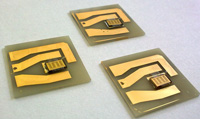
Picture: IMEC’s SiN/AlGaN/GaN FET.
GaN compounds are the best candidates to replace silicon power devices due to their high bandgap energy (giving excellent transport properties) and their high electrical breakdown field. However, the cost of GaN power devices is high. Nevertheless, GaN epilayers grown on large-diameter silicon wafers (potentially up to 200mm) offer a lower-cost technology compared to other substrates.
By growing an SiN/AlGaN/GaN/AlGaN double-heterostructure FET structure on a silicon substrate and combining it with in-situ SiN grown in the same epitaxial sequence as the III-nitride layers, the research institute has obtained enhancement-mode (E-mode) device operation (which is typically required in applications for safety reasons).
Device fabrication is based on an optimized process for the selective removal of in-situ SiN. The resulting SiN/AlGaN/GaN/AlGaN double-heterostructure FET is characterized by a high breakdown voltage of almost 1000V (980V), excellent uniformity, and a low dynamic specific on-resistance of 3.5mW.cm2 that is well within the present state-of-the-art, says IMEC. The results hold the promise of a large market opportunity for GaN-on-Si power devices, the research institute reckons.
Within its industrial affiliation program (IIAP) on GaN-on-Si technology (launched in July), IMEC and its partners are focusing on the development of GaN technology for both power conversion and solid-state lighting applications. A key goal is to lower GaN technology cost by using large-diameter GaN-on-Si and hence by leveraging economies of scale. IMEC invites both integrated device manufacturers and the compound semiconductor industry to join the program, adding that partners can build on its expertise in GaN as well as benefiting from sharing costs, risk and talent.
See related item:
IMEC launches industrial affiliation program on GaN-on-Si technology
![]() Search: IMEC FET GaN Silicon substrates
Search: IMEC FET GaN Silicon substrates
Visit: www.imec.be
![]() ©2009 Juno Publishing and Media Solutions Ltd. All rights reserved. Semiconductor Today and the editorial material contained within it and related media is the copyright of Juno Publishing and Media Solutions Ltd. Reproduction in whole or part without permission from Juno Publishing and Media Solutions Ltd is forbidden. In most cases, permission will be granted, if the author, magazine and publisher are acknowledged.
©2009 Juno Publishing and Media Solutions Ltd. All rights reserved. Semiconductor Today and the editorial material contained within it and related media is the copyright of Juno Publishing and Media Solutions Ltd. Reproduction in whole or part without permission from Juno Publishing and Media Solutions Ltd is forbidden. In most cases, permission will be granted, if the author, magazine and publisher are acknowledged.
Disclaimer: Material published within Semiconductor Today and related media does not necessarily reflect the views of the publisher or staff. Juno Publishing and Media Solutions Ltd and its staff accept no responsibility for opinions expressed, editorial errors and damage/injury to property or persons as a result of material published.
Semiconductor Today, Juno Publishing and Media Solutions Ltd, Suite no. 133, 20 Winchcombe Street, Cheltenham, GL52 2LY, UK
Web site by No Name No Slogan ![]()