| Home | About Us | Contribute | Bookstore | Advertising | Subscribe for Free NOW! |
| News Archive | Features | Events | Recruitment | Directory |
| FREE subscription |
| Subscribe for free to receive each issue of Semiconductor Today magazine and weekly news brief. |
News
23 December 2009
Direct wafer bond route to III-V field-effect transistors
Japanese researchers have been developing direct wafer bonding (DWB) to transfer III-V semiconductor-on-insulator (III-V-OI) materials onto silicon with a view to creating new field-effect transistors to replace silicon complementary metal-oxide-semiconductor (CMOS) devices [Masafumi Yokoyama et al, Appl. Phys. Express, vol2, p124501, 2009]. The research team consists of scientists from the University of Tokyo, Japan’s National Institute of Advanced Industrial Science and Technology (NAIST), and Sumitomo Chemical.
While DWB has been used to create optoelectronic devices on silicon, the creation of III-V transistors using the technique faces a number of challenges. To compete with coming ultra-thin-body silicon-on-insulator (SOI) CMOS, the III-V materials would have to be incorporated into a similar format. Ultra-thin-body III-V material quality is very sensitive to damage created by the bonding process. Further problems arise in creating suitably doped source/drain (S/D) regions.
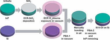
Figure 1: DWB process for integrating thin-body III-V-OI channel layer on a Si wafer. PBA-1 and PBA-2: pre-bonding annealing and post-bonding annealing, respectively.
The researchers worked with one of the most promising materials for nMOSFETs – indium gallium arsenide (InGaAs). Metal-organic chemical vapor deposition (MOCVD) was used to grow a 100nm-thick layer of In0.53Ga0.47As on a 2-inch diameter indium phosphide (InP) wafer (Figure 1). The insulating buried silicon dioxide (BOX) layer was grown on top of the InGaAs using electron cyclotron resonance (ECR) plasma sputtering. The ECR process was chosen over traditional plasma-enhanced chemical vapor deposition (PECVD) as giving better controllability and atomic-level flatness (a root-mean-square surface roughness of about 0.2nm) when used on III-V semiconductor material. By growing the BOX on the InGaAs before bonding, one can maintain a good InGaAs/BOX interface. An oxygen plasma treatment is used to further enhance the bonding energy between the BOX and the silicon substrate. The silicon and BOX/InGaN/InP wafers were then bonded manually in air. The InP wafer was then removed using a (1000:1 InP:InGaAs) selective etch in hydrogen chloride solution, leaving the InGaAs surface layer.
Among the characterizations of the resulting InGaAs layer, it was found that the Hall (electron) carrier mobility was ~7000cm2/V-s, which compares reasonably with a bulk InGaAs value of ~11,000cm2/V-s. The mobility of electrons in bulk silicon is about 1500cm2/V-s.
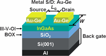 Figure 2: Schematic of metal S/D thin-body III-V-OI nMOSFET on Si wafer with back-gate.
The DWB III-V material was used to create back-gated III-V-OI MOSFETs (Figure 2). The S/D consisted of gold-germanium contacts, while the gate was aluminum deposited on the back side of the silicon. The gate length at this stage is a massive 500μm (state-of-the-art silicon is pressing on downward to 32nm and smaller). The channel width was 100μm.
The effective mobility in the resulting nMOSFETs was measured at 1200cm2/V-s, corresponding to a 1.9x enhancement factor over comparable silicon nMOSFETs.
The researchers conclude: “These results indicate that the present DWB technique is quite promising for integrating ultra-thin-body or multi-gate III-V-OI MOSFETs on the silicon CMOS platform as the ultimate CMOS transistors.”
![]() Search: InGaAs
Search: InGaAs
Visit: http://apex.ipap.jp/link?APEX/2/124501/
The author Mike Cooke is a freelance technology journalist who has worked in the semiconductor and advanced technology sectors since 1997.
![]() ©2009 Juno Publishing and Media Solutions Ltd. All rights reserved. Semiconductor Today and the editorial material contained within it and related media is the copyright of Juno Publishing and Media Solutions Ltd. Reproduction in whole or part without permission from Juno Publishing and Media Solutions Ltd is forbidden. In most cases, permission will be granted, if the author, magazine and publisher are acknowledged.
©2009 Juno Publishing and Media Solutions Ltd. All rights reserved. Semiconductor Today and the editorial material contained within it and related media is the copyright of Juno Publishing and Media Solutions Ltd. Reproduction in whole or part without permission from Juno Publishing and Media Solutions Ltd is forbidden. In most cases, permission will be granted, if the author, magazine and publisher are acknowledged.
Disclaimer: Material published within Semiconductor Today and related media does not necessarily reflect the views of the publisher or staff. Juno Publishing and Media Solutions Ltd and its staff accept no responsibility for opinions expressed, editorial errors and damage/injury to property or persons as a result of material published.
Semiconductor Today, Juno Publishing and Media Solutions Ltd, Suite no. 133, 20 Winchcombe Street, Cheltenham, GL52 2LY, UK
Web site by No Name No Slogan ![]()