| Home | About Us | Contribute | Bookstore | Advertising | Subscribe for Free NOW! |
| News Archive | Features | Events | Recruitment | Directory |
| FREE subscription |
| Subscribe for free to receive each issue of Semiconductor Today magazine and weekly news brief. |
News
14 December 2009
NEC reports GaN-on-Si power transistor with high threshold voltage control
At last week’s International Electron Devices Meeting (IEDM 2009) in Baltimore, MD, USA (7–9 December), Tokyo-based NEC Corp and NEC Electronics Corp presented the development of a nitride power transistor on a silicon (Si) substrate that has improved normally-off characteristics (the control and suppression of electrical currents when voltage is not applied — a necessary feature for the safe operation of consumer electronics and IT devices).
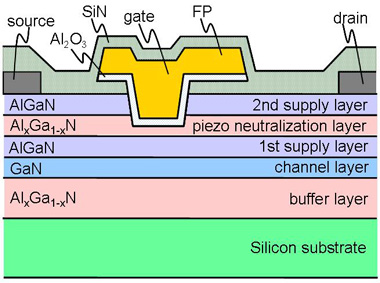
Figure: Cross-sectional view of NEC's GaN-on-Si power transistor.
The transistor features a new structure for the layer beneath the gate electrode, which improves the controllability of threshold voltage that intercepts electrical currents, enabling the realization of low power losses, high-speed switching and high-temperature operations, says the firm.
NEC says that, although power transistors using silicon have a key role in advancing energy conserving as they convert electrical power and serve as a controlling element for applications ranging from consumer electronics to industrial machinery, expectations are high for the implementation of nitride transistors, which demonstrate lower-level losses, higher speeds and higher-temperature operations compared with existing silicon transistors. However, it is important to suppress variations in threshold voltage and to improve the reproducibility of their normally-off characteristics, the firm stresses.
In existing transistors composed of a two-layer structure consisting of an aluminum nitride gallium (AlGaN) electron supply layer and a gallium nitride (GaN) channel layer, a great deal of variation in threshold voltage occurs due to differences in the thickness of the AlGaN electron supply layer under the gate, which is etched down from 20–30nm to just a few nanometers in order to achieve normally-off characteristics. A high-precision etching process is particularly needed to reduce the variation in threshold voltage and to stabilize the normally-off characteristics.
A five-layer structure enables NEC's new transistors to control the threshold voltage with a high degree of precision by reducing its dependence on the thickness of the electron supply layer. This is accomplished by introducing an electric charge neutralization layer (the ‘piezo’ neutralization layer) within the electron supply layer, while also introducing a buffer layer — beneath the channel layer — with the same composition as the piezo neutralization layer. This structure enables uniform manufacturing of nitride semiconductor power transistors that realize normally-off characteristics at a low cost. The transistors also exhibit low power loss and high breakdown voltage, the firm adds.
NEC says that it aims to accelerate its R&D towards the design, evaluation and implementation of nitride power transistors.
![]() Search: NEC GaN power transistor Silicon substrates
Search: NEC GaN power transistor Silicon substrates
Visit: www.nec.co.jp
![]() ©2009 Juno Publishing and Media Solutions Ltd. All rights reserved. Semiconductor Today and the editorial material contained within it and related media is the copyright of Juno Publishing and Media Solutions Ltd. Reproduction in whole or part without permission from Juno Publishing and Media Solutions Ltd is forbidden. In most cases, permission will be granted, if the author, magazine and publisher are acknowledged.
©2009 Juno Publishing and Media Solutions Ltd. All rights reserved. Semiconductor Today and the editorial material contained within it and related media is the copyright of Juno Publishing and Media Solutions Ltd. Reproduction in whole or part without permission from Juno Publishing and Media Solutions Ltd is forbidden. In most cases, permission will be granted, if the author, magazine and publisher are acknowledged.
Disclaimer: Material published within Semiconductor Today and related media does not necessarily reflect the views of the publisher or staff. Juno Publishing and Media Solutions Ltd and its staff accept no responsibility for opinions expressed, editorial errors and damage/injury to property or persons as a result of material published.
Semiconductor Today, Juno Publishing and Media Solutions Ltd, Suite no. 133, 20 Winchcombe Street, Cheltenham, GL52 2LY, UK
Web site by No Name No Slogan ![]()