| Home | About Us | Contribute | Bookstore | Advertising | Subscribe for Free NOW! |
| News Archive | Features | Events | Recruitment | Directory |
| FREE subscription |
| Subscribe for free to receive each issue of Semiconductor Today magazine and weekly news brief. |
News
15 December 2009
First InGaAs FinFETs suppress short-channel effects
Purdue University is claiming the first ‘well behaved’ inversion-mode (i.e. normally-off) indium gallium arsenide FinFET (a field-effect transistor with a fin structure) with a gate length down to 100nm [Y.Q. Wu et al, International Electron Devices Meeting (IEDM 2009), session 13.4, 8 December]. The gate dielectric was aluminum oxide (Al2O3), grown using atomic layer deposition (ALD) techniques. The fin height was 40nm.
The researchers report much better control of short-channel effects (SCEs), compared with normal planar InGaAs MOSFET transistors, in terms of electro-static control, resulting in improved sub-threshold slope (SS, 34% better with 100nm gate length, compared with planar device), drain induced barrier lowering (DIBL, reduced from 480mV/V to 180mV/V) and threshold voltage (VT) roll-off (about 30% that of a planar device), along with less degradation of these properties at raised temperature (up to 360K).
In related work, Purdue has developed a new hydrogen bromide (HBr) pre-treatment, along with retro-grade channel structuring and halo-implantation, to improve the InGaAs/high-k dielectric interface for planar MOSFETs [Y.Q. Wu et al, IEDM 2009, session 13.2, 8 December]. The work on both the FinFET and the planar MOSFET was led by Purdue doctoral student Yanqing Wu.
Transistors using InGaAs have been proposed as solving (for a time) many of the problems raised by the continuous shrinking of CMOS devices on silicon. The higher mobility of InGaAs compared with silicon leads to larger currents in the on-state. However, off-state performance needs to be much improved to meet the requirements of the International Technology Roadmap for Semiconductors (ITRS). Off-state short-channel effects in InGaAs kick in much faster due to its narrower bandgap and higher dielectric constant (k), compared with silicon.
Wrap-around gate structures, such as the fin channels in FinFETs, provide better control of the off-state. This requires highly challenging etch processes with low surface damage and a good interface with high-k gate dielectrics. Dry (plasma) etch of III-V materials such as InGaAs can be particularly tricky.
Although the ultimate aim would be to create InGaAs FinFETs on silicon substrates with diameters up to 300mm and beyond, the Purdue researchers used a 2-inch indium phosphide (InP) substrate for the ‘proof-of concept’ device (Figure 1). The device layers were grown using molecular beam epitaxy (MBE). A heavily doped InP layer was grown beneath the In0.53Ga0.47As channel to reduce punch-through of current in the off-state and current leakage through the substrate. One negative effect of the high doping was worse junction leakage due to the non-optimized contacts that were used.
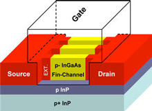 Figure 1:
Schematic of Purdue’s InGaAs FinFET.
Figure 1:
Schematic of Purdue’s InGaAs FinFET.
An Al2O3 dielectric ‘encapsulation layer’ was then grown to a thickness of 10nm using an ASM F-120 reactor. The source and drain regions were created using selective ion implantation of silicon through the dielectric into the InGaAs. Rapid thermal annealing (RTA) was performed to mend the InGaAs crystal structure damaged by the implantation and thus to activate the silicon doping.
The fin structures were created by using a combination of wet and dry etch techniques, resulting in damage-free sidewalls. The dry etch was performed using a boron trichloride (BCl3)/argon (Ar) plasma. An electron-beam lithography resist (ZEP-520A) was used as a mask for the etch process. The surface layer damaged by the dry etch was removed using a 3 second dip in a dilute sulfuric acid/hydrogen peroxide (H2SO4:H2O2:H2O) solution. The researchers believe a more sophisticated process is needed to create more vertical side-walls (Figure 2).
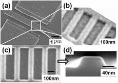 Figure 2. Tilted SEM image of FinFET device. (b) Zoomed-in image of channel region covered with gate dielectric and metal. (c) SEM image of the fin structure after dry etching. (d) Cross section SEM image of fin after dry etching.
The Al2O3 encapsulation was removed with a buffered-oxide etch (BOE) solution. The Al2O3 dielectric was re-grown as a 5nm gate dielectric film after an ammonium sulfide ((NH4)2S) surface preparation. Electron-beam evaporation and lift-off was used to form the source/drain contacts using AuGe/Ni/Au layers. The gate was Ni/Au, created similarly.
The improved sub-threshold slope (SS) is taken as an indicator of the ‘damage-free’ nature of the etch process of the fin. Normally, for planar devices the interface trap density can be estimated from the variation of SS values with temperature. Since the FinFET cannot have better surface quality than the planar device, the better overall SCE behavior must impact the SS performance. However, the very good SS values obtained do indicate high-quality interfaces, enabling the researchers to declare that the dry/wet etch process is ‘damage free’. By making suitable extrapolations, the Purdue team estimates an upper limit on the average interface trap density (Dit) of 1.7x10¹²/cm2-eV.
In addition, in work yet to be published, the Purdue researchers also claim to be the first to grow hafnium dioxide (HfO2) dielectric on fin-structures. Such a dielectric is among the leading contenders for use as high-k dielectric on traditional CMOS transistors. Companies such as Intel and IBM have both proposed its use.
![]() Search: InGaAs FinFET ALD MBE InP substrates
Search: InGaAs FinFET ALD MBE InP substrates
Visit: https://engineering.purdue.edu
The author Mike Cooke is a freelance technology journalist who has worked in the semiconductor and advanced technology sectors since 1997.
![]() ©2009 Juno Publishing and Media Solutions Ltd. All rights reserved. Semiconductor Today and the editorial material contained within it and related media is the copyright of Juno Publishing and Media Solutions Ltd. Reproduction in whole or part without permission from Juno Publishing and Media Solutions Ltd is forbidden. In most cases, permission will be granted, if the author, magazine and publisher are acknowledged.
©2009 Juno Publishing and Media Solutions Ltd. All rights reserved. Semiconductor Today and the editorial material contained within it and related media is the copyright of Juno Publishing and Media Solutions Ltd. Reproduction in whole or part without permission from Juno Publishing and Media Solutions Ltd is forbidden. In most cases, permission will be granted, if the author, magazine and publisher are acknowledged.
Disclaimer: Material published within Semiconductor Today and related media does not necessarily reflect the views of the publisher or staff. Juno Publishing and Media Solutions Ltd and its staff accept no responsibility for opinions expressed, editorial errors and damage/injury to property or persons as a result of material published.
Semiconductor Today, Juno Publishing and Media Solutions Ltd, Suite no. 133, 20 Winchcombe Street, Cheltenham, GL52 2LY, UK
Web site by No Name No Slogan ![]()