| Home | About Us | Contribute | Bookstore | Advertising | Subscribe for Free NOW! |
| News Archive | Features | Events | Recruitment | Directory |


News
29 December 2009
Fluorine enhanced AlGaN HEMTs
Researchers at Xidian University in China have compared the effectiveness of different fluorine plasma treatments in achieving enhancement-mode (normally off) nitride semiconductor high electron mobility transistors (HEMTs) using a fluorine plasma treatment [Quan Si et al, J. Semicond., vol30, p124002, 2009].
Normally, HEMTs produced using combinations of aluminum gallium nitride (AlGaN) tend to operate in depletion-mode (normally on). Although depletion mode devices can be used to produce useful circuits, electronics based on enhancement mode devices tend to waste much less power. The ubiquity of silicon-based complementary metal-oxide-semiconductor (CMOS) electronics is based in part on the ease with which enhancement mode devices can be built using that technology.
Enhancement-mode AlGaN HEMTs could make for energy efficient circuit options that operate at high power, frequency and/or temperature. Applications for which AlGaN HEMT technology (even in depletion-mode) is being developed include power amplifiers for wireless communications network base-stations (up to ~40GHz) and inverters for conversion between DC and AC power in electric and hybrid vehicles. The development of enhancement-mode devices in the technology could extend its reach into more complex devices that include logic.
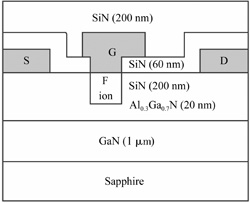 Figure 1: Schematic cross section of enhancement-mode AlGaN/GaN HEMT.
Fluorine plasma treatment has been one of the methods used in recent times to shift the threshold voltage of AlGaN into the enhancement-mode region (Figure 1). The Xidian researchers used step-and-repeat lithography and reactive ion etch to separately expose regions of the same AlGaN/GaN wafer to four different 150 second plasma treatments with carbon tetrafluoride (CF4) in the reactive ion etch chamber (Figure 2). This avoids the performance differences that can arise from devices built of different wafers.
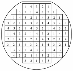 Figure 2: The arrangement of plasma treatments on the AlGaN/GaN wafer. Region 1 corresponds to conventional HEMT devices with no plasma treatment. Regions 2-4 were subjected to plasma treatments of 150 seconds with powers of 55W, 150W and 250W, respectively.
The AlGaN/GaN layers were grown on sapphire using metal-organic chemical vapor deposition (MOCVD). The AlGaN layer contained 30% AlN. The final 0.6μm gate length HEMTs had source/drain regions with ohmic contacts and a Schottky gate.
The effect of the plasma treatment was to shift the threshold voltage upwards from the negative value achieved without plasma treatment (region 1). As the plasma power increases, the fluorine ion (F-)density and kinetic energy increases. This means that the fluorine penetrates to greater depth in the AlGaN barrier below the gate region, coming closer to the GaN channel. However, higher power (150W) plasma treatment also damages the performance of the device in terms of reduced electron mobility in the channel. At the highest plasma power tested (250W), the fluorine ions reach the channel, killing electron mobility.
The threshold shift with a plasma power of 150W is sufficient to result in enhancement-mode operation with some impact on electron mobility, compared with normal depletion-mode HEMTs. The peak current density was 501mA/mm and the peak transconductance was 210mS/mm. The threshold voltage was +0.57V. The etch damage resulted in a peak transconductance smaller than that of traditional GaN HEMTs.
It was found that gate leakage under forward bias was comparable to that of conventional devices, while the reverse bias leakage was reduced in plasma treated devices, indicating an increased tunneling width. A final effect of the 150W plasma treatment was reduced extrinsic cut-off and maximum oscillation frequencies in small-signal RF measurements (Table 1).
Plasma power |
fT |
fmax |
W |
GHz |
GHz |
0 |
20.9 |
31.6 |
55 |
21.3 |
32.4 |
150 |
19.4 |
26 |
Table 1: Measured extrinsic cut-off (fT) and maximum oscillation (fmax) frequencies for three different plasma treated devices. A plasma power of ‘0W’ represents ‘no plasma treatment’.
![]() Search: AlGaN HEMT
Search: AlGaN HEMT
Visit: http://dx.doi.org
The author Mike Cooke is a freelance technology journalist who has worked in the semiconductor and advanced technology sectors since 1997.
![]() ©2009 Juno Publishing and Media Solutions Ltd. All rights reserved. Semiconductor Today and the editorial material contained within it and related media is the copyright of Juno Publishing and Media Solutions Ltd. Reproduction in whole or part without permission from Juno Publishing and Media Solutions Ltd is forbidden. In most cases, permission will be granted, if the author, magazine and publisher are acknowledged.
©2009 Juno Publishing and Media Solutions Ltd. All rights reserved. Semiconductor Today and the editorial material contained within it and related media is the copyright of Juno Publishing and Media Solutions Ltd. Reproduction in whole or part without permission from Juno Publishing and Media Solutions Ltd is forbidden. In most cases, permission will be granted, if the author, magazine and publisher are acknowledged.
Disclaimer: Material published within Semiconductor Today and related media does not necessarily reflect the views of the publisher or staff. Juno Publishing and Media Solutions Ltd and its staff accept no responsibility for opinions expressed, editorial errors and damage/injury to property or persons as a result of material published.
Semiconductor Today, Juno Publishing and Media Solutions Ltd, Suite no. 133, 20 Winchcombe Street, Cheltenham, GL52 2LY, UK
Web site by No Name No Slogan ![]()