| Home | About Us | Contribute | Bookstore | Advertising | Subscribe for Free NOW! |
| News Archive | Features | Events | Recruitment | Directory |
| FREE subscription |
| Subscribe for free to receive each issue of Semiconductor Today magazine and weekly news brief. |
News
8 July 2009
Osaka Uni claims first red electro-luminescence from MOCVD Eu-doped GaN LEDs
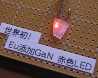 Researchers at Japan's Osaka University have demonstrated what is claimed to be the first low-voltage operation of current-injected red light emission from a p-type/Eu-doped/n-type GaN LED at room temperature (Nishikawa et al, Appl. Phys. Express 2 (2009) 071004).
Trivalent ions of the rare-earth element europium (Eu3+) have been widely used as phosphors (doped into an insulator) to yield red light emission (by optical excitation) in cathode ray-tube and plasma display panels. Previous researchers have doped Eu into the gallium nitride by using ion implantation with post-thermal annealing or molecular-beam epitaxy, and then used optical excitation to stimulate red light emission in LEDs. However, such rare-earth-doped semiconductors are expected to produce highly efficient electroluminescent devices as a result of the specific optical properties of the materials (e.g. sharp, intense and temperature-independent emission due to the intra-4f shell energy transitions of electrons in the atom).
Red electroluminescence has been obtained from indium–tin-oxide (ITO)/Eu-doped GaN/undoped GaN grown on p-type silicon substrates and metal–insulator–semiconductor (MIS) structures of indium (In)/Eu-doped GaN/undoped GaN grown on n-type silicon. However, the applied voltage was as high as 46V for the ITO/Eu-doped GaN sample and the emission efficiency was low for the In/Eu-doped GaN sample because the impact excitation of the Eu3+ ions by hot carriers was thought to be dominant. To reduce the operation voltage, it is necessary to use a p–n junction diode structure to inject current into the active layer.
Since metal-organic chemical vapor deposition (MOCVD) has been used widely to fabricate commercially available blue LEDs, MOCVD-grown Eu-doped GaN inserted into a p–n junction diode structure should yield high electroluminescent efficiency. A difficulty in MOCVD growth of Eu-doped GaN is the lack of a suitable metal-organic source for the Eu-dopant. However, the vapor pressure of most candidate Eu sources is generally much lower than that of conventional metal-organic sources so, when transporting the Eu source to the reactor chamber, special precautions are needed (e.g. high-temperature heating of the transfer lines to avoid condensation and/or low-pressure control of the cylinder to supply a certain amount of the source).
Now, led by Yasufumi Fujiwara (professor in the Graduate School of Engineering’s Division of Materials and Manufacturing Science) the Osaka group says that it has overcome these problems and used MOCVD to grow light-emitting Eu-doped GaN layers in a p-type/Eu-doped/n-type GaN LED structure on a sapphire substrate. The growth temperature was optimized at 1050ºC (the same as for the undoped GaN layer between the LED structure and the GaN buffer/sapphire substrate) but a lower V/III ratio of 320 was required to obtain strong emission intensity (compared with 1600 for the undoped GaN layer).
Electrical current injection using an applied voltage as low as 3V yielded red emission that was easily visible to the naked eye under normal lighting conditions. At a dc drive current of 20mA, the output power - integrated over the dominant 5D0–7F2 intra-4f shell transition in Eu3+ ions (about 621nm) - was 1.3µW. The corresponding external quantum efficiency was 0.001%.
The excitation mechanism for Eu3+ luminescence is thought to involve the excitation energy being transferred from the host GaN material to the 5D3 state of the Eu3þ ion and successive nonradiative (phonon) relaxation occurring from the higher 5DJ>0 states to the 5D0 state. No GaN-related luminescence was observed, indicating that the excitation energy of the GaN host material was effectively transferred to the Eu3+ ions for Eu-related luminescence.
Increasing the applied voltage caused the emission intensity to increase. However, the color also changed slightly from red to orange (attributed to color mixing of the main emission peak with an emerging emission peak at 543nm, due to the higher spectral sensitivity of the human eye for emission at 543nm).
Although the optical output is still small, Fujiwara reckons that it is possible to boost the output by optimizing the electrode structure and other features of the LED.
The researchers say that their result suggests a novel method for realizing GaN-based red LEDs (an alternative to conventional toxic As-containing AlGaInP/GaAs red LEDs). In addition, such red GaN-based LEDs could be integrated monolithically with existing green and blue GaN-based LEDs on the same substrate to form red-green-blue (RGB) devices, for use in solid-state lighting or full-color displays (e.g. with smaller pixel size and a higher resolution).
![]() Search: GaN LEDs MOCVD Sapphire substrate
Search: GaN LEDs MOCVD Sapphire substrate
Visit: www.mat.eng.osaka-u.ac.jp
Visit: http://apex.ipap.jp/link?APEX/2/071004
![]() ©2009 Juno Publishing and Media Solutions Ltd. All rights reserved. Semiconductor Today and the editorial material contained within it and related media is the copyright of Juno Publishing and Media Solutions Ltd. Reproduction in whole or part without permission from Juno Publishing and Media Solutions Ltd is forbidden. In most cases, permission will be granted, if the author, magazine and publisher are acknowledged.
©2009 Juno Publishing and Media Solutions Ltd. All rights reserved. Semiconductor Today and the editorial material contained within it and related media is the copyright of Juno Publishing and Media Solutions Ltd. Reproduction in whole or part without permission from Juno Publishing and Media Solutions Ltd is forbidden. In most cases, permission will be granted, if the author, magazine and publisher are acknowledged.
Disclaimer: Material published within Semiconductor Today and related media does not necessarily reflect the views of the publisher or staff. Juno Publishing and Media Solutions Ltd and its staff accept no responsibility for opinions expressed, editorial errors and damage/injury to property or persons as a result of material published.
Semiconductor Today, Juno Publishing and Media Solutions Ltd, Suite no. 133, 20 Winchcombe Street, Cheltenham, GL52 2LY, UK
Web site by No Name No Slogan ![]()