| Home | About Us | Contribute | Bookstore | Advertising | Subscribe for Free NOW! |
| News Archive | Features | Events | Recruitment | Directory |
| FREE subscription |
| Subscribe for free to receive each issue of Semiconductor Today magazine and weekly news brief. |
News
27 November 2009
Fuji Electric smoothes way to silicon carbide power transistors
Japan’s Fuji Electric Device Technology has been researching the digging of U-shape trenches in silicon carbide (SiC) with a view to next-generation power transistor technology [Yasuyuki Kawada, Jpn. J. Appl. Phys., vol48, p116508, 2009].
Although technological development has produced improved pure-silicon power devices such as superjunction metal-oxide-semiconductor field-effect transistors (SJ-MOSFET) and field-stop insulated-gate bipolar transistors (FS-IGBT), SiC is expected to eventually produce superior results for blocking voltages, on-resistance and operating frequencies.
Accessing these new levels of performance would enable more efficient power consumption, more compact equipment and less active cooling requirements. SiC Schottky diodes are already commercially available, and a number of demonstrations of SiC transistor devices and circuits have been made by various companies and research groups.
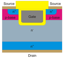 Power devices often use vertical trench-shaped structures to reduce on-resistance compared with traditional planar designs (see Figure 1). U-shaped trenches are particularly favored, since rounded structures reduce the peak electric field and hence the breakdown of the device. However, producing trenches in SiC is a particularly difficult process since the material has a hardness approaching that of diamond. It also has a very stable chemical structure.
Figure 1 (above): Metal-oxide-semiconductor field-effect transistor with U-shaped gate (UMOSFET).
Plasma etching (dry etch) of SiC is a very slow process. Even at high plasma density, etch rates are of the order of a couple of microns an hour. An additional difficulty for the U-shape trenches that are needed for power devices is that one needs a very smooth surface with no sharp angles. This is hard to achieve with dry etch – in fact, some groups follow up a dry process with a slower wet chemical etch to create a smooth surface finish.
The Fuji group has studied an alternative to this – annealing at high temperatures up to 1800°C. The SiC was etched using SF6/O2/Ar gas chemistry in an inductively coupled plasma process. The trench patterns were made with a silicon dioxide (SiO2) mask that was patterned with photoresist and then subjected to a reactive ion etch to reach the SiC substrate. Once the trenches had been produced, the SiO2 was removed with a wet chemical etch.
Trench depths of 3-8μm were produced. The substrate was a 4H polytype with a c-face (8° off-axis). The trench directions were chosen to give sidewalls consisting of [1_110x] and [_1110x] faces. The annealing duration was varied between 1 minute and 2 hours in a horizontal hot-wall reactor originally designed for SiC epitaxy. Various atmospheres were applied during the process: pure argon (Ar), silane-argon (SiH4-0.09%Ar), or hydrogen (H2). Pressures varied from 1.5 to 720 Torr.
 After a wide-ranging investigation, the Fuji group concluded that a SiH4/Ar anneal at high temperature is useful for obtaining rounded trench corners without significant etching, while H2 at the low end of the temperature range that was studied is an effective way to obtain a smooth substrate surface without changing the trench shape. The best pressure was found to be about 80 Torr.
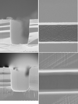
Figure 2: Cross-sectional (left) and plane-view (right) scanning electron microscope (SEM) images of trenches without (a) and with (b) two-step annealing, first at 1700°C in SiH4/Ar (10min) and then 1500°C in H2 (10min).
The Fuji team therefore proposes a two-step anneal process: first at 1700°C in SiH4/Ar to round the trench corners, and then at 1500°C in H2 to smooth the SiC surfaces (Figure 2). The group believes that its results are comparable with what is achievable with silicon trench technology. The mechanism behind the transformations achieved by these annealing processes is believed to be surface diffusion and evaporation–condensation.
See related item:
SiC electronics needs transistor stimulus
![]() Search: SiC SiC power transistors
Search: SiC SiC power transistors
Visit: http://jjap.ipap.jp/link?JJAP/48/116508
Visit: www.fujielectric.co.jp/eng/fdtThe author Mike Cooke is a freelance technology journalist who has worked in the semiconductor and advanced technology sectors since 1997.
![]() ©2009 Juno Publishing and Media Solutions Ltd. All rights reserved. Semiconductor Today and the editorial material contained within it and related media is the copyright of Juno Publishing and Media Solutions Ltd. Reproduction in whole or part without permission from Juno Publishing and Media Solutions Ltd is forbidden. In most cases, permission will be granted, if the author, magazine and publisher are acknowledged.
©2009 Juno Publishing and Media Solutions Ltd. All rights reserved. Semiconductor Today and the editorial material contained within it and related media is the copyright of Juno Publishing and Media Solutions Ltd. Reproduction in whole or part without permission from Juno Publishing and Media Solutions Ltd is forbidden. In most cases, permission will be granted, if the author, magazine and publisher are acknowledged.
Disclaimer: Material published within Semiconductor Today and related media does not necessarily reflect the views of the publisher or staff. Juno Publishing and Media Solutions Ltd and its staff accept no responsibility for opinions expressed, editorial errors and damage/injury to property or persons as a result of material published.
Semiconductor Today, Juno Publishing and Media Solutions Ltd, Suite no. 133, 20 Winchcombe Street, Cheltenham, GL52 2LY, UK
Web site by No Name No Slogan ![]()