| Home | About Us | Contribute | Bookstore | Advertising | Subscribe for Free NOW! |
| News Archive | Features | Events | Recruitment | Directory |
| FREE subscription |
| Subscribe for free to receive each issue of Semiconductor Today magazine and weekly news brief. |
News
27 November 2009
Thickening aluminum nitride layers on sapphire substrates
Japan’s Mie University has been investigating various ways to deposit thick layers of aluminum nitride (AlN) on sapphire substrates using hydride vapor phase epitaxy (HVPE) [Jiejun Wu et al, Appl. Phys. Express, vol.2, p.111004, 2009].
The research group believes AlN is promising as the basis for ultraviolet (UV) LEDs and high-electron-mobility transistors (HEMTs). UV radiation has important medical applications and, in combination with suitable phosphors, could be used as the driver of white-light modules.
However, thick AlN layers are difficult to grow with the high quality that is needed for such applications. In the x-ray diffraction characterization of such layers, some peaks can have full-width at half maximum (FWHM) values of ~1000arcsec, indicating poor quality.
In fact, the large FWHMs in AlN layers seem to arise from edge-type threading dislocations (TDs), as indicated by the asymmetric (10.2) and (10.0) planes giving rise to broad reflection peaks, while symmetric ones such as (00.2) can be as small as 100arcsec. Edge TDs have a far bigger impact on device performance compared with screw TDs.
Epitaxial lateral over-growth and related techniques have been used to decrease densities of TDs in both GaN and AlN layers. However, these techniques are complex and expensive. The Mie group therefore wants to develop simple methods for growing thick AlN layers.
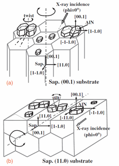 As a preliminary to this, the researchers sought to understand the reasons for the dislocations. First, growing c-plane AlN on c-plane sapphire allows the initial islands of AlN crystal material to be twisted relative to each other. When these islands coalesce, edge TDs can occur (Figure 1, top).
Growing c-plane AlN on a-plane sapphire (making the two c-axes perpendicular) reduces this twisting effect (Figure 1, bottom). While the tendency for neighboring AlN islands to have different out-of-plane tilts is increased, this can be controlled with suitable optimization of growth temperature and III/V element ratios.
Figure 1 (above): Schematics of twist and tilt variations between AlN islands grown on c-plane (a) and a-plane (b) sapphire.
The researchers also comment that a-plane sapphire has a smaller lattice mismatch with AlN and that easy cleavage along the r-plane would be convenient for the construction of laser diode facets.
The researchers used HVPE at low pressure (5kPa) to grow c-plane AlN on c-plane (00.1) and on a-plane (11.0) sapphire. The material sources were ammonia (NH3), Al and hydrogen chloride (HCl). The sapphire surface was prepared with a thermal clean in hydrogen for 10 minutes at 1150°C. The AlN was grown at 1350-1550°C. No buffers or interlayers were used. Optimized conditions for AlN growth varied for the different sapphire orientations: for (00.1)/c-plane sapphire, 1400°C with a V/III ratio of 200; for (11.0)/a-plane, 1500°C with the V/III ratio set at 600.
The resulting XRD measurements suggest a lower edge-type TD density for the a-plane sapphire growth, although the screw TD density increased somewhat. In particular, the asymmetric (10.2) and (10.0) peaks had FWHMs of 487 and 636arcsec, respectively, for the a-plane sapphire grown sample, while the c-plane sample recorded 752 and 927arcsec, respectively. The symmetric (00.2) reflection was 312arcsec for the a-plane sample, but only 176arcsec for the c-plane sample.
From these figures, the Mie group derives a rough estimate for edge and screw TD densities of 2.7x10⁸ and 2.6x10⁷/cm2, respectively, for the a-plane sample, and 5.8x10⁸ and 8.1x10⁶/cm2, respectively, for the c-plane sample. It was also found that the window for off-optimum growth while maintaining reasonable crystal structure was wider for the a-plane compared with c-plane growth.
The researchers also studied cracking effects in the AlN layer. They were able to maintain crack-free AlN growth on a-plane sapphire beyond 3.6μm thickness (Figure 2), while cracks appeared in material grown on c-plane sapphire at 1.8μm. Cracking did occur on a-plane sapphire with a 4μm-thick AlN layer, but the density of cracks (25.5/cm) was a factor of five lower than that for the 1.8μm layer on c-plane sapphire (145.9/cm).
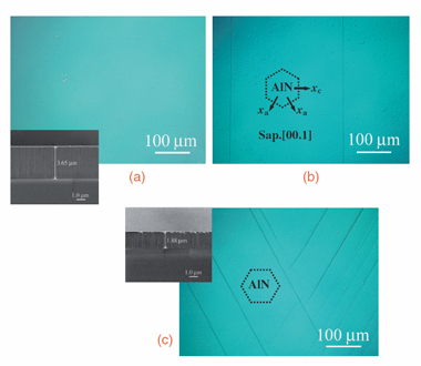
Figure 2: Optical microscope images of AlN grown on a-plane sapphire: crack-free 3.6μm layer (a), and cracking in a slightly thicker 4μm layer (b). On c-plane sapphire, a relatively thin 1.8μm layer exhibits cracks (c).
The a-plane sapphire sample showed cracks in only one direction, which the Mie researchers explain in terms of the larger thermal expansion coefficient of sapphire parallel to the c-axis, compared with the perpendicular direction.
![]() Search: AlN Sapphire substrates HVPE
Search: AlN Sapphire substrates HVPE
Visit: http://apex.ipap.jp/link?APEX/2/111004/
The author Mike Cooke is a freelance technology journalist who has worked in the semiconductor and advanced technology sectors since 1997.
![]() ©2009 Juno Publishing and Media Solutions Ltd. All rights reserved. Semiconductor Today and the editorial material contained within it and related media is the copyright of Juno Publishing and Media Solutions Ltd. Reproduction in whole or part without permission from Juno Publishing and Media Solutions Ltd is forbidden. In most cases, permission will be granted, if the author, magazine and publisher are acknowledged.
©2009 Juno Publishing and Media Solutions Ltd. All rights reserved. Semiconductor Today and the editorial material contained within it and related media is the copyright of Juno Publishing and Media Solutions Ltd. Reproduction in whole or part without permission from Juno Publishing and Media Solutions Ltd is forbidden. In most cases, permission will be granted, if the author, magazine and publisher are acknowledged.
Disclaimer: Material published within Semiconductor Today and related media does not necessarily reflect the views of the publisher or staff. Juno Publishing and Media Solutions Ltd and its staff accept no responsibility for opinions expressed, editorial errors and damage/injury to property or persons as a result of material published.
Semiconductor Today, Juno Publishing and Media Solutions Ltd, Suite no. 133, 20 Winchcombe Street, Cheltenham, GL52 2LY, UK
Web site by No Name No Slogan ![]()