| Home | About Us | Contribute | Bookstore | Advertising | Subscribe for Free NOW! |
| News Archive | Features | Events | Recruitment | Directory |
| FREE subscription |
| Subscribe for free to receive each issue of Semiconductor Today magazine and weekly news brief. |
News
9 October 2009
Squeezing light out of silicon
National Taiwan University (NTU) in Taipei has been working on combining silicon (Si), silicon dioxide (SiO2) and zinc oxide (ZnO) to create light emitting structures using nanocrystals [Edward Sun et al, Nanotechnology, vol.20, p.445202, 2009]. While the external quantum efficiency of up to 4.3x10⁻⁴ (0.043%) at 1150nm wavelength is not that impressive when compared against standard light emitting devices with efficiencies of tens of percent, the fact is that silicon-based technology does not give up photons lightly. However, this external quantum efficiency is two orders of magnitude greater than that of a comparison bulk Si device.
Silicon is the most widely used material for electronics, solar cells, and also has broad application to photonic devices using its structuring properties to create waveguides, modulators, etc. In terms of light emission, silicon’s Achilles heel is its indirect bandgap – the bottom of its conduction band does not line up with the top of the valence band when presented in crystal momentum (k) space.
Simple light emission in semiconductors requires a transition from a state in the conduction band to a hole in the valence band of essentially the same k, since photons have effectively zero k. This is only easily achievable in “direct” semiconductors such as gallium arsenide (GaAs) and nitride (GaN), where the bottom of the conduction band lines up with the top of valence band.
Indirect semiconductors like silicon can be used in the reverse direction where photons are absorbed pushing an electron up from the valence band (leaving a hole) to the conduction band directly above. The excited electron then loses energy thermally to end up near the bottom of the conduction band.
For light emission in Si, one has to depend on “phonon-assisted” transitions to enable a suitable shift in k-space. Since this requires an extra coupling to phonons (vibrational levels), the rate for such processes is usually much reduced compared with the interaction in direct semiconductors.
It is hoped that Si can be coaxed into emitting if the right combination of structures can be found, such as superlattices (repeating layers of material that create new band behaviors), nanocrystals (creating new electron levels), nano-patterning, etc. In addition, complementary materials such as better transparent conductive oxides (TCOs) could increase the light output.
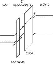 The NTU researchers used different Si-nanocrystal structures, with a silicon dioxide matrix and aluminum-doped ZnO as TCO (Figure 1). The aluminum increases the electron concentrations, adding to the n-type conduction behavior of ZnO, making it an attractive low-cost TCO candidate. (If a system to create effective p-type behavior in ZnO were found, it might also be a new source for creating direct bandgap white-light LEDs, like GaN.)
Figure 1: Schematic band diagram of the n-ZnO/SiO2–Si nanocrystals-SiO2/p-Si heterojunction LED at forward bias. The injected electrons and holes recombine to produce light in the Si nanocrystals.
In NTU’s work on nanocrystal Si emission, the n-ZnO is used as a source of electrons for injection into the nanocrystals through a tunneling process (Figure 1), while the holes come from the p-type Si substrate.
Different structures were used to test the various measures implemented to increase light output (Figure 2). The researchers also investigated the anti-reflective effects of the TCO layer thickness to increase light output. The SiO2 matrix layers above and below the nanocrystals were designed to provide further confinement of the electron levels in the nanocrystals, along with surface passivation.
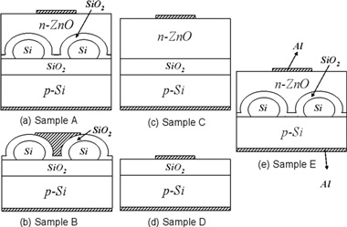
Figure 2: Schematic of various structures tested at NTU: (a) sample A: Al/n-ZnO/SiO2–Si nanocrystals- SiO2/p-Si/Al, (b) sample B: Al/SiO2–Si nanocrystals-SiO2/p-Si/Al, (c) sample C: Al/n-ZnO/SiO2/p-Si/Al, (d) sample D: Al/SiO2/p-Si/Al, (e) sample E: Al/n-ZnO/SiO2–Si nanocrystals/p-Si/Al (without the oxide layer underneath the nanocrystals).
The 35nm-diameter hemi-spherical grain nanocrystals were created in a low-pressure chemical vapor deposition (LPCVD, 0.25Torr at 550°C) with a post-deposition thermal oxidation. The spacing between the nanocrystals was about 45nm, giving a density of 8.1 × 109cm-2. The TCO was grown using atomic layer deposition.
The NTU team comments that the turn-on voltage of 3.6V is low enough for integration with silicon microelectronics and that the processes used are compatible with standard ultra-large-scale Si-based semiconductor production. They hope that their work will eventually lead to the fabrication of efficient Si LEDs for silicon-based photonic applications.
Since the external light emission was from the edges around the aluminum electrodes, it was estimated that the internal quantum efficiency of the best device (sample A) was around 10-3 or 0.1%. The comparison bulk Si LED (sample D) had an external quantum efficiency of around 5x10⁻⁶.
![]() Search: ZnO
Search: ZnO
Visit: www.iop.org/EJ/abstract
The author Mike Cooke is a freelance technology journalist who has worked in the semiconductor and advanced technology sectors since 1997.
![]() ©2009 Juno Publishing and Media Solutions Ltd. All rights reserved. Semiconductor Today and the editorial material contained within it and related media is the copyright of Juno Publishing and Media Solutions Ltd. Reproduction in whole or part without permission from Juno Publishing and Media Solutions Ltd is forbidden. In most cases, permission will be granted, if the author, magazine and publisher are acknowledged.
©2009 Juno Publishing and Media Solutions Ltd. All rights reserved. Semiconductor Today and the editorial material contained within it and related media is the copyright of Juno Publishing and Media Solutions Ltd. Reproduction in whole or part without permission from Juno Publishing and Media Solutions Ltd is forbidden. In most cases, permission will be granted, if the author, magazine and publisher are acknowledged.
Disclaimer: Material published within Semiconductor Today and related media does not necessarily reflect the views of the publisher or staff. Juno Publishing and Media Solutions Ltd and its staff accept no responsibility for opinions expressed, editorial errors and damage/injury to property or persons as a result of material published.
Semiconductor Today, Juno Publishing and Media Solutions Ltd, Suite no. 133, 20 Winchcombe Street, Cheltenham, GL52 2LY, UK
Web site by No Name No Slogan ![]()