| Home | About Us | Contribute | Bookstore | Advertising | Subscribe for Free NOW! |
| News Archive | Features | Events | Recruitment | Directory |
| FREE subscription |
| Subscribe for free to receive each issue of Semiconductor Today magazine and weekly news brief. |
News
28 October 2009
Stimulating development in UV AlGaN emission
Sheffield University researchers have improved stimulated 340nm ultraviolet (UV) emission from aluminum gallium nitride (AlGaN) multi-quantum well (MQW) structures [Wang et al, App. Phys. Lett., vol.95, p161904, 2009]. The tests so far have been carried out using optical pumping, with thresholds as low as 6.6kW/ cm2, but the team believes that their structures could lead to a simple electrical pumping UV (including deep UV/DUV) laser diode (LD) scheme.
The 340nm range of wavelengths has important applications in investigating biomolecules. Present technology uses bulky harmonic generation equipment to reach the high electromagnetic frequencies of UV. A UV laser diode could create opportunities for portable equipment. In principle, the AlGaN material system covers wavelengths between 364nm a photon energy of about 3.4eV for the band gap of GaN) and 200nm (~6.2eV for the band gap of AlN).
One obstruction for progressing to stable AlGaN LDs presently consists of poor crystal quality. A further difficulty arises from the lattice mismatches between high-Al-content AlGaN and the GaN layer that is commonly used as the buffer between sapphire substrate and the electronic III-nitride structures. The mismatch can lead to tensile stress and thus cracking in the device layers. Removing this block is the focus of Sheffield’s latest published research.
Using AlN as part of the buffer structure could improve the situation. Unfortunately, the optimal temperature for AlN is far above that achievable in normal semiconductor production equipment. The AlN layers that can be grown have high dislocation densities. In this situation, many groups have resorted to complicated epitaxial lateral overgrowth (ELOG) methods to produce material with the reduced crystal dislocation densities needed for UV LDs.
Last year, Hamamatsu used a hetero-facet controlled epitaxial lateral overgrowth (hetero-FACELO) technique to achieve electrically pumped lasers with wavelengths of 336nm [Harumasa Yoshida et al, Appl. Phys. Lett., vol.93, p241106, 2008] and 342nm [Harumasa Yoshida et al, Nature Photonics vol.2, p551, 2008]. In 2006, the University of South Carolina reported on the use of a patterned lateral overgrowth (PLOG) to achieve 214nm stimulated emission from a high-quality AlN layer under optical pumping [Shatalov et al, Jpn. J. Appl. Phys., vol. 45, pL1286, 2006]. Commercial devices produced using ELOG are available that emit around 375nm.
However, ELOG and related approaches are difficult to apply to AlGaN. Another way is to use silicon carbide substrates to produce III-nitride devices, but the base material is extremely expensive.
Since 2005, the Sheffield group has developed two techniques leading to improved AlGaN crystal layers on sapphire with a view to UV and DUV emission. The latest research is the first time the team has applied its techniques to laser emission.
Two sets of samples on sapphire substrates were produced (Figure 1): one (‘thin GaN interlayer’) had a 0.5μm layer of flat aluminum nitride (AlN) and then 12nm or 100nm of gallium nitride (GaN); the other had 0.3-0.5μm of porous AlN and then 0.2-0.3μm of flat AlN. Both structures were then topped off with 1μm of Al0.29Ga0.71N before Al0.16Ga0.84N/Al 0.05Ga0.95N MQWs were applied. The porous AlN method can be repeated to improve quality further.
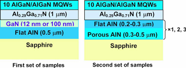
Figure 1: Schematics of various structures used to investigate stimulated UV emission from AlGaN.
Low-pressure metal-organic chemical vapor deposition (LP-MOCVD) was used to grow the layers on 2-inch sapphire substrates. All layers on this occasion were undoped, presumably because the aim at this stage was to study optically pumped stimulated emission. The growth of the flat AlN was carried out at 1200°C; the porous AlN at 1150°C; and, the GaN interlayers at 1130°C. The porous AlN samples were varied in the number of repeats from one to three.
Inspection for cracking of the MQW structures revealed small amounts towards the edges for the 100nm GaN interlayer sample and for the sample with a double porous AlN structure. With three repeats of the porous AlN, cracking appeared between the edge and the middle of the sample. The researchers are investigating the causes of cracking such as temperature-non-uniformities induced by wafer bowing. Samples with 12nm GaN interlayer, the single repeat of the porous AlN structure, and a reference 1μm AlN layer showed no cracking.
Crystal quality evaluations of the porous AlN samples showed narrower ‘rocking curves’ for x-ray diffraction with increased number of repeats. Narrower rocking curves indicate better crystal quality. The rocking curve full-width of half maximum (FWHM) for the reference AlN layer sample was ~1300arcsec, but going to three repeats of the porous AlN reduced this to ~580arcsec. The researchers estimate that corresponding dislocation densities are 2.0x10¹⁰/cm2 and 3.2x10⁹/cm2, respectively.
Despite the cracking, stimulated emission was achieved with the 100nm GaN interlayer, but not with 12nm. The optical pumping density for stimulated emission was 7.7kW/cm2. With the thin interlayer, stimulated emission did not occur at pumping up to 15kW/cm2. The pump laser was a pulsed diode-pumped neodymium doped yttrium aluminum garnet laser (266nm wavelength, pulse repetition 850Hz, pulse width 9nsec).
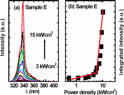 The porous AlN samples only showed stimulated emission for the three-repeat sample, at 6.6kW/cm2 (Figure 2). The researchers comment that this threshold is lower than other reports and attribute the achievement to the significant improvement in AlN crystal quality leading to better optical confinement.
Figure 2: Emission spectra (a, edge emission) and integrated intensity vs. optical pumping power (b) for sample using three repeats of porous AlN as buffer layer.
![]() Search: UV AlGaN multi-quantum well
Search: UV AlGaN multi-quantum well
Visit: http://link.aip.org/link/?APPLAB/95/161904/1
Visit: www.nature.com/nphoton
Visit: http://link.aip.org/link/?APPLAB/93/241106/1
Visit: http://jjap.ipap.jp/link?JJAP/45/L1286/
The author Mike Cooke is a freelance technology journalist who has worked in the semiconductor and advanced technology sectors since 1997.
![]() ©2009 Juno Publishing and Media Solutions Ltd. All rights reserved. Semiconductor Today and the editorial material contained within it and related media is the copyright of Juno Publishing and Media Solutions Ltd. Reproduction in whole or part without permission from Juno Publishing and Media Solutions Ltd is forbidden. In most cases, permission will be granted, if the author, magazine and publisher are acknowledged.
©2009 Juno Publishing and Media Solutions Ltd. All rights reserved. Semiconductor Today and the editorial material contained within it and related media is the copyright of Juno Publishing and Media Solutions Ltd. Reproduction in whole or part without permission from Juno Publishing and Media Solutions Ltd is forbidden. In most cases, permission will be granted, if the author, magazine and publisher are acknowledged.
Disclaimer: Material published within Semiconductor Today and related media does not necessarily reflect the views of the publisher or staff. Juno Publishing and Media Solutions Ltd and its staff accept no responsibility for opinions expressed, editorial errors and damage/injury to property or persons as a result of material published.
Semiconductor Today, Juno Publishing and Media Solutions Ltd, Suite no. 133, 20 Winchcombe Street, Cheltenham, GL52 2LY, UK
Web site by No Name No Slogan ![]()