| Home | About Us | Contribute | Bookstore | Advertising | Subscribe for Free NOW! |
| News Archive | Features | Events | Recruitment | Directory |
News
9 April 2010
Leti demos fully CMOS-compatible laser source coupled to silicon waveguide
Leti of Grenoble, France, the Laboratory for Electronics & Information Technology of the French government's research and technology organization CEA, has demonstrated a fully CMOS-compatible laser source coupled to a silicon waveguide, which is claimed to be a major milestone toward the WADIMOS project’s goal of fabricating silicon photonics circuits in CMOS foundries for an optical network-on-chip (optoNoC).
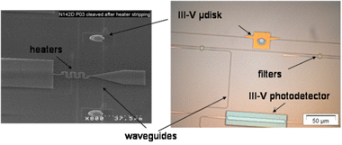
Picture: Microdisk laser, detector and passive routing circuitry.
WADIMOS (Wavelength Division Multiplexed Photonic Layer on CMOS) is a three-year EU-funded research project (with a total budget of €3.2m) that started in January 2008 and aims to demonstrate a photonic interconnect layer on CMOS. The project is coordinated by international research center IMEC of Leuven, Belgium, which is designing ultra-compact SOI (silicon-on-insulator) waveguide circuits for routing and demultiplexing, as well as contributing to fabrication of the sources and their integration with the waveguides.
Leti’s role is to develop the integration process and fabricate the photonic layer, including the III-V based microsources, in a standard CMOS pilot line. Other project partners include European chip-maker STMicroelectronics (which is investigating the viability of optical networks-on-chip and is designing the required CMOS circuits), MAPPER Lithography (a spin-off of Holland’s Delft University that is developing a massively parallel e-beam writing system, and is responsible for the system studies related to the terabit optical link), INL–Lyon Institute of Nanotechnology (which is involved in the design and fabrication of the microsource arrays, as well as contributing to the optoNoC system studies, and is responsible for designing the optical routers), and UNITN–Trento University (which is designing optical WDM circuits based on coupled ring resonators).
WADIMOS partners will present the results at next week’s SPIE Photonics Europe 2010 event in Brussels, Belgium (12–16 April).
Working with a circuit design from INL and Imec, Leti completed the specific process studies for the laser source to adapt and modify standard III-V materials process steps that would comply with a CMOS environment, replacing gold-based metal contacts with a Ti/TiN/AlCu metal stack.
Leti says that the enormous computing power of multi-processor systems and manufacturing tools being considered will require data transfer rates of more than 100Terabit/s. These data rates may be needed on-chip, e.g. in multi-core processors, which are expected to require total on-chip data rates of up to 100TB/s by 2015, or off-chip, e.g. in short-distance data interconnects, requiring up to 100TB/s over a distance of 10–100m. Optical interconnects are the only viable technology for transmitting these amounts of data, Leti asserts.
Besides a huge data rate, optical interconnects also allow for additional flexibility through the use of wavelength division multiplexing (WDM). This feature may help to realize more intelligent interconnect systems such as the optical network-on-chip system that the WADIMOS project is also investigating.
WADIMOS aims to build a complex photonic interconnect layer incorporating multi-channel microsources, microdetectors and different advanced wavelength-routing functions directly integrated with electronic driver circuits. It also aims to demonstrate the application of such electro-photonic ICs in two representative applications: an on-chip optical network and a terabit optical datalink.
![]() Search: Leti
Search: Leti
Visit: http://wadimos.intec.ugent.be
![]() ©2010 Juno Publishing and Media Solutions Ltd. All rights reserved. Semiconductor Today and the editorial material contained within it and related media is the copyright of Juno Publishing and Media Solutions Ltd. Reproduction in whole or part without permission from Juno Publishing and Media Solutions Ltd is forbidden. In most cases, permission will be granted, if the author, magazine and publisher are acknowledged.
©2010 Juno Publishing and Media Solutions Ltd. All rights reserved. Semiconductor Today and the editorial material contained within it and related media is the copyright of Juno Publishing and Media Solutions Ltd. Reproduction in whole or part without permission from Juno Publishing and Media Solutions Ltd is forbidden. In most cases, permission will be granted, if the author, magazine and publisher are acknowledged.
Disclaimer: Material published within Semiconductor Today and related media does not necessarily reflect the views of the publisher or staff. Juno Publishing and Media Solutions Ltd and its staff accept no responsibility for opinions expressed, editorial errors and damage/injury to property or persons as a result of material published.
Semiconductor Today, Juno Publishing and Media Solutions Ltd, Suite no. 133, 20 Winchcombe Street, Cheltenham, GL52 2LY, UK
Web site by No Name No Slogan ![]()