| Home | About Us | Contribute | Bookstore | Advertising | Subscribe for Free NOW! |
| News Archive | Features | Events | Recruitment | Directory |
News
1 April 2010
Capacity of InGaAs to increase drive current in nano MOSFETs
Many in the semiconductor industry and the supporting research community are seeking to apply compound semiconductor materials to improve metal-oxide semiconductor (MOS) field-effect transistor (FET) performance. These workers are particularly attracted by the increased electron mobilities of some III-V compound semiconductor materials, such as those in the indium gallium arsenide (InGaAs) system.
With other factors being equal, increased mobility would lead to increased transistor performance. This being the real world, other factors are not equal. A particular one that has recently come to prominence is that high-mobility materials tend to have a lower density of electron states. This leads to a reduced ability of gate potentials to increase electron densities in the channel, turning transistor devices on for drive current flow.
A number of groups are working on this problem. The Yale University Center for Research on Interface Science and Phenomena (CRISP) has recently published its simulations for the resulting drive current potential in InGaAs, along with the more traditional silicon and germanium [Abigail Lubow et al, Appl. Phys. Lett., vol96, p122105, 2010], based on the completed PhD work of Dr Abigail Lubow.
Since nano-scale devices are being targeted, effects that were previously unimportant have come to prominence. One such problem is the distribution of charge carriers at the oxide-semiconductor interface. In larger devices, this can be treated as a two-dimensional sheet. For future nano-devices, a sheet thickness of a few nanometers could kill performance (Figure 1). A shift in the centroid of charge away from the gate potential adds to the equivalent oxide thickness (EOT), reducing the inversion capacitance.
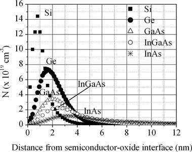
Figure 1: Electron carrier concentration in silicon and four high-mobility channel materials as a function of distance from the oxide-semiconductor interface for EOT = 1nm and Vg–Vt = 1.4V. As density of states decreases, the charge centroid moves further from the oxide–semiconductor interface.
Simulations based on a Schrodinger–Poisson model suggest that there is indeed a reduction of capacitance in higher-mobility materials (Figure 2). Many experimental studies do not show such a reduction; an effect that is probably due to charging/discharging of interface traps masking the centroid shift. Reducing interface trap densities to less than 1011/cm2 should reveal the reduction in capacitance in high-mobility materials, the Yale researchers believe.
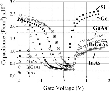
Figure 2: Capacitance–voltage curves for Si/Ge/GaAs/InGaAs/InAs in the nMOS device for EOT=1nm and Vg–Vt=1.4V. Quantum effects cause a reduction in inversion capacitance.
Despite this, the Yale researchers suggest that the drive current in the on-state could be increased by up to 9.8x, compared with silicon, in InAs for n-type MOS transistors (nMOS, with negative-charge ‘electron’ carriers) — see Table 1. For pMOS (with positive-charge ‘hole’ carriers), there is little advantage in the III-V InGaAs system, but germanium-based channels could achieve a 3.9x drive current, compared with silicon. However, achieving this level of performance depends on finding suitable gate dielectric materials.
μ |
Cinv |
μ Cinv |
Id ratio |
|
cm2/V-s |
x10-6F/cm2 |
X10-3F/V-s |
||
Si |
1350 |
2.62 |
3.53 |
1 |
Ge |
3600 |
2.50 |
9.01 |
2.5 |
GaAs |
8000 |
1.67 |
13.3 |
3.7 |
InGaAs |
11200 |
1.44 |
16.1 |
4.5 |
InAs |
30000 |
1.16 |
34.9 |
9.8 |
Table 1: Mobility (μ), inversion capacitance (Cinv), and expected nMOS drive current (Id) ratios for EOT=1nm and Vg−Vt=1.4V.
Other research groups have also been looking at quantum and centroid effects on inversion capacitance with a view to III-V logic. The MIT group under Jésus del Alamo presented a model at the International Electron Devices Meeting (IEDM) in December 2009 [D. Jin et al, session 20.4; also see short report on this in Mike Cooke, Semiconductor Today, February 2009, p116] for quantum gate capacitance effects. This work was applied to describing experiments involving Schottky-gate high-electron-mobility transistor (HEMT) devices, rather than with insulated-gate MOSFETs.
Visit: http://link.aip.org
The author Mike Cooke is a freelance technology journalist who has worked in the semiconductor and advanced technology sectors since 1997.

![]() ©2010 Juno Publishing and Media Solutions Ltd. All rights reserved. Semiconductor Today and the editorial material contained within it and related media is the copyright of Juno Publishing and Media Solutions Ltd. Reproduction in whole or part without permission from Juno Publishing and Media Solutions Ltd is forbidden. In most cases, permission will be granted, if the author, magazine and publisher are acknowledged.
©2010 Juno Publishing and Media Solutions Ltd. All rights reserved. Semiconductor Today and the editorial material contained within it and related media is the copyright of Juno Publishing and Media Solutions Ltd. Reproduction in whole or part without permission from Juno Publishing and Media Solutions Ltd is forbidden. In most cases, permission will be granted, if the author, magazine and publisher are acknowledged.
Disclaimer: Material published within Semiconductor Today and related media does not necessarily reflect the views of the publisher or staff. Juno Publishing and Media Solutions Ltd and its staff accept no responsibility for opinions expressed, editorial errors and damage/injury to property or persons as a result of material published.
Semiconductor Today, Juno Publishing and Media Solutions Ltd, Suite no. 133, 20 Winchcombe Street, Cheltenham, GL52 2LY, UK
Web site by No Name No Slogan ![]()