| Home | About Us | Contribute | Bookstore | Advertising | Subscribe for Free NOW! |
| News Archive | Features | Events | Recruitment | Directory |
News
3 August 2010
China makes 120nm HEMTs with cut-offs above 100GHz
Researchers based in China have developed 120nm III-V high-electron-mobility transistors (HEMTs) with millimeter-wave broadband and satellite communication applications in mind [Huang Jie et al, J. Semicond., vol31, p074008, 2010]. The current-gain cut-off frequency (fT) was 141GHz and the maximum power gain cut-off was (fmax) 120GHz.
The research was carried out by scientists from Chinese Academy of Sciences’ Institute of Microelectronics and China’s Southwest University in Chongqing. The researchers see their new indium gallium arsenide/indium aluminum arsenide (InGaAs/InAlAs) devices as being “promising in millimeter-wave devices and integrated circuits”.
The device structures (Table 1) were grown on semi-insulating indium phosphide (InP) substrates using molecular beam epitaxy (MBE). To make the transistors, the source and drain regions were formed first using the deposition and lift-off of six layers of alloyed metal (nickel, germanium, gold, germanium, nickel, gold). The resulting contact resistance was measured at 0.2Ω-mm using the transmission line model (TLM).
Si doping/cm3 |
|||
In0.53Ga0.47As |
Cap |
30nm |
1x10¹⁹ |
InP |
Etch stop |
6nm |
|
In0.52Al0.48As |
Barrier |
10nm |
|
Planar Si- δ-doped |
5x10¹² |
||
In0.52Al0.48As |
Spacer |
3nm |
|
In0.7Ga0.3As |
Channel |
10nm |
|
In0.52Al0.48As |
Buffer |
300nm |
|
SI InP substrate |
Table 1: InGaAs/InAlAs HEMT epitaxial layer structure.
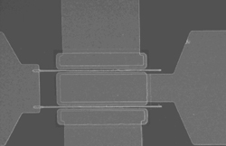 The mesa isolation structures were formed by a wet chemical etch using an aqueous solution of phosphate (H3PO4) and hydrogen peroxide. Electron-beam evaporation was used to create the titanium-gold wiring (Figure 1).
Figure 1: Partial photograph of the InGaAs/InAlAs HEMT.
To produce short gate lengths of ~100nm, the researchers developed a four-layer electron-beam resist process – poly(methyl methacrylate) (PMMA), polymethylglutarimide (PMGI), ZEP520, polymethylglutarimide (PMGI). ZEP520 is a high-performance resist developed by Zeon Corp of Japan. The China researchers report that use of the bottom PMGI layer helps in the clean removal of the resist layers compared with a structure that has a ZEP520 bottom layer.
The gate (Figure 2) was recessed into the cap layer with a wet citric acid/hydrogen peroxide etch that was stopped by an InP etch-stop layer (selectivity InGaAs/InP ~160). The gate metal consisted of titanium, platinum and gold, which was deposited in an evaporation and lift-off process. A T-gate shape was used to reduce parasitic capacitance and resistance effects. The gate had a 120nm length and a 2x50μm width. Passivation was not used because the researchers wanted to avoid increasing the gate capacitance and thus impact the high-frequency performance.
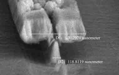
Figure 2: SEM photo of T-shaped pattern of the InGaAs/InAlAs HEMT.
In DC operation, the HEMT’s saturation drain-to-source current was found to be 446mA/mm. The maximum extrinsic transconductance (Gm) of 520mS/mm was obtained under conditions where the gate-source voltage was –0.5V and the drain-source voltage was 1.5V. Subthreshold, the gate leakage – a little less than 0.1μA – is dominated by current from the drain. The pinch-off/threshold voltage is –1V (hence the transistor is ‘on’ at 0V).
The frequency performance was extracted from measurements made in the range 0.1–26.1GHz. The maximum power gain cut-off was determined from measurements made at a drain–source voltage of 1.5V and a gate–source voltage of –0.5V. Parasitic effects were de-embedded from the measurements.
![]() Search: HEMTs InP substrates
Search: HEMTs InP substrates
Visit: http://iopscience.iop.org
The author Mike Cooke is a freelance technology journalist who has worked in the semiconductor and advanced technology sectors since 1997.
![]() ©2010 Juno Publishing and Media Solutions Ltd. All rights reserved. Semiconductor Today and the editorial material contained within it and related media is the copyright of Juno Publishing and Media Solutions Ltd. Reproduction in whole or part without permission from Juno Publishing and Media Solutions Ltd is forbidden. In most cases, permission will be granted, if the author, magazine and publisher are acknowledged.
©2010 Juno Publishing and Media Solutions Ltd. All rights reserved. Semiconductor Today and the editorial material contained within it and related media is the copyright of Juno Publishing and Media Solutions Ltd. Reproduction in whole or part without permission from Juno Publishing and Media Solutions Ltd is forbidden. In most cases, permission will be granted, if the author, magazine and publisher are acknowledged.
Disclaimer: Material published within Semiconductor Today and related media does not necessarily reflect the views of the publisher or staff. Juno Publishing and Media Solutions Ltd and its staff accept no responsibility for opinions expressed, editorial errors and damage/injury to property or persons as a result of material published.
Semiconductor Today, Juno Publishing and Media Solutions Ltd, Suite no. 133, 20 Winchcombe Street, Cheltenham, GL52 2LY, UK
Web site by No Name No Slogan ![]()