| Home | About Us | Contribute | Bookstore | Advertising | Subscribe for Free NOW! |
| News Archive | Features | Events | Recruitment | Directory |
News
16 August 2010
Unveiling hot-electron over-spill in nitride LEDs
Researchers at the US Virginia Commonwealth University and Lithuania’s Semiconductor Physics Institute believe that hot electrons may be more important in nitride light-emitting diodes (LEDs) than previously considered [X. Ni et al, J. Appl. Phys., vol108, p033112, 2010]. In line with their ideas, they have developed LED structures that reduce these effects and improve light emission efficiency.
Normally, nitride LEDs are modeled with electrons that are in thermal equilibrium with their immediate surroundings. For this to be an accurate representation, the electrons need to interact with these surroundings as they enter the active region. If instead the electrons do not interact, they will be ‘hot’ and will cross the active region at a higher energy than expected and could even spill over into the p-contact region where they recombine (Figure 1), most-likely without radiating light, or with unwanted parasitic wavelengths.
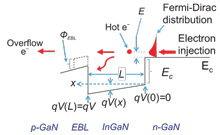 Figure 1: Schematic of electron overflow caused by ballistic or quasi-ballistic transport across InGaN active region. Hot electrons can traverse the active region ballistically and quasi-ballistically, avoiding recombination inside InGaN (contributing to the electron overflow), or be thermalized and captured inside the active region through interactions with LO phonons.
Such hot or ‘ballistic’ electrons are also less likely to be blocked by electron-blocking layers (EBLs) that are commonly a feature of such devices designed to reduce over-spill. The researchers’ models also suggest that ‘quasi-ballistic’ electrons that have undergone only one interaction with a longitudinal optical (LO) phonon could also contribute to overflow into the p-contact.
“We would like to underscore that consideration of hot electrons, and their ballistic and quasiballistic transport across the active region, is revolutionary when it comes to light emitters such as those discussed here,” the researchers comment.
Electron–phonon interactions in nitride semiconductors are particularly strong due to the more ionic nature of bonds in the crystal. This means that LO phonons, rather than acoustic phonons, form the main route to thermalization in high electric fields.
To test their ideas and models, the researchers grew a series of double-heterostructure LED structures. Some were produced on free-standing m-plane GaN supplied by Kyma Technologies using low-pressure metal-organic chemical vapor deposition (MOCVD); others were grown on c-plane sapphire. The active region of the m-plane devices consisted of 6nm of undoped In0.2Ga0.8N, giving a peak wavelength of ~440nm (blue). The c-plane active region consisted of 6nm of undoped In0.15Ga0.85N with peak wavelength ~410nm (violet).
The active layers of both device types were followed by a 3nm undoped In0.01Ga0.99N layer. Before these layers (i.e. on the n-side of the diode), a silicon-doped In0.01Ga0.99N underlayer was used. Various heights of electron blocking were used by varying the aluminum content in a 10nm AlxGa1-xN layer (x = 0%, 8% or 15%) deposited before the magnesium-doped p-GaN contact (~100nm).
Devices with and without a three-level staircase electron injector (SEI) were produced (Figure 2). The SEI consisted of 5nm layers of n-InGaN with In compositions of 3%, 6% and 10% before the active region. The first step from the 1% In underlayer was very close to or smaller than the energy of the ~88meV longitudinal optical phonon assumed to be responsible for thermalization.
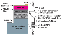 Figure 2: Schematic for two m-plane LEDs with InGaN SEI before active regions. The SEI is designed to thermalize injected electrons from n-GaN layers. Devices with and without EBL were compared.
To avoid degradation of the material quality by the insertion of the SEI, a six-period multi-quantum well (MQW) was incorporated into the underlayer.
The epitaxial materials were processed into LEDs with 250μm-diameter mesa formation and contact metal deposition. The tests were carried out with pulsed operation to avoid self-heating effects that degrade performance. The detection geometry was kept the same throughout the experiments, but not all photons were collected so the results indicated relative efficiencies only.
Without the SEI, the EBL had a big effect in increasing the relative external quantum efficiency of the devices: the devices without an EBL had EQEs reduced by a factor of three to five. However with the SEI there was little difference in the emissions with or without an EBL in the m-plane device set-up (Figure 3). This is taken as indicative that only negligible thermionic emission remains to allow electrons to cross the barrier (i.e. the SEI arrangement has successfully thermalized the electron distribution).
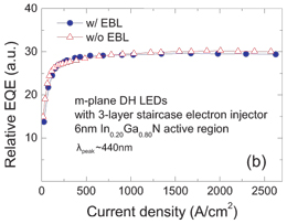 Figure 3. Relative EQE of two m-plane LEDs with SEI, with and without EBL (pulsed current, 1μsec pulse width, 0.1% duty cycle).
With the c-plane devices with SEI there is some difference in behavior but not at the level shown by device without an SEI (Figure 4). The researchers note: “Somewhat unexpectedly, in the c-plane case the LED without EBL shows even higher EQE than that with the EBL when the current density is below 1700A/cm2.”
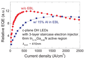 Figure 4. Relative EQE of two c-plane LEDs with SEI inserted under active region: with and without EBLs (pulsed current, 1μsec pulse width, 0.1% duty cycle).
The reduced EQE above 1700A/cm2 is attributed to factors such as ‘current filamentation’ (inhomogeneity perpendicular to the direction of current flow). Also, the EBL may block the holes from entering the active region due to their heavier effective mass and low concentration in the c-plane case. The degradation in performance of the device without EBL above 500A/cm2 may also suggest that the c-plane orientation may require more thermalization to avoid electron overflow due to polarization field effects.
The researchers suggest that these results should also be applicable to the design of laser diodes where high threshold current densities make the carrier thermalization an even more important issue.
Visit: http://link.aip.org
Visit: www.pfi.lt/index_e.html
The author Mike Cooke is a freelance technology journalist who has worked in the semiconductor and advanced technology sectors since 1997.
![]() ©2010 Juno Publishing and Media Solutions Ltd. All rights reserved. Semiconductor Today and the editorial material contained within it and related media is the copyright of Juno Publishing and Media Solutions Ltd. Reproduction in whole or part without permission from Juno Publishing and Media Solutions Ltd is forbidden. In most cases, permission will be granted, if the author, magazine and publisher are acknowledged.
©2010 Juno Publishing and Media Solutions Ltd. All rights reserved. Semiconductor Today and the editorial material contained within it and related media is the copyright of Juno Publishing and Media Solutions Ltd. Reproduction in whole or part without permission from Juno Publishing and Media Solutions Ltd is forbidden. In most cases, permission will be granted, if the author, magazine and publisher are acknowledged.
Disclaimer: Material published within Semiconductor Today and related media does not necessarily reflect the views of the publisher or staff. Juno Publishing and Media Solutions Ltd and its staff accept no responsibility for opinions expressed, editorial errors and damage/injury to property or persons as a result of material published.
Semiconductor Today, Juno Publishing and Media Solutions Ltd, Suite no. 133, 20 Winchcombe Street, Cheltenham, GL52 2LY, UK
Web site by No Name No Slogan ![]()