- News
13 December 2010
Power, speed and other highlights of IEDM 2010
The past few years have seen growing interest in using nitride semiconductors as components in power systems. The wide bandgaps (> 3.4eV) of gallium nitride (GaN) and aluminum gallium nitride (AlGaN) mean that the breakdown electric field is large compared with more traditional semiconductors such as silicon (Si) or gallium arsenide (GaAs). The wider bandgap also allows such devices to maintain their performance characteristics to higher temperatures.
This year’s International Electron Devices Meeting (IEDM) last week (6–8 December 2010) had a special focus on power electronics, where gallium nitride technologies were to the fore. The themes of these presentations were energy efficiency and supply for green technologies.
Session 13 was titled ‘Emerging Technologies – Next Generation Power Devices and Technology’, while ‘Advanced Power Devices and Reliability’ from the perspective of quantum and compound semiconductor technology was also the topic of session 20.
The earlier of these sessions was concerned mainly with sifting through potential applications and matching them to suitable potential technologies. Applications include battery control (e.g. switching and charging), motors (e.g. in hybrid electric vehicles, industrial processes etc), renewable energy distribution into the electric grid, etc.
For many of these uses, silicon is the favored option due to its long development and low cost. However, some companies such as Toyota (session 13.5) and consultant Dr Michael A. Briere of ACOO Enterprises LLC (13.6) see potential for the application of GaN and silicon carbide (SiC) to automotive, and even voltage regulator modules for multi-processor CPU power control. Some key features of these devices are higher power efficiencies and higher power densities.
Session 20 reported actual structures and technologies for high-power/voltage operation, mainly in nitride semiconductors, but also with some silicon technology. Some of the nitride research is aimed at characterizing traps that can impact performance [Ohio State University, Wright Patterson Air Force Base, Wyle Labs, 20.1], or looking for degradation mechanisms [MIT, 20.2; IMEC, University of Padova, 20.3; Hong Kong University of Science and Technology, Nitronex, 20.4] of nitride high-electron-mobility transistors (HEMTs).
MIT found that RF stress created more degradation compared with a comparable DC voltage. IMEC and Padova applied for the first time the time-dependent dielectric breakdown (TDDB) technique that is used in CMOS reliability assessments to give lifetime extrapolations.
HKUST et al reported the on-state reliability of HEMTs that were treated with fluorine plasma to shift the threshold voltage to ‘enhancement mode’, i.e. normally-off operation that is desirable for lower power consumption. A critical voltage was found that seemed to be caused by impact ionization of the fluorine ions in the barrier layer.
Also, new high-power device structures were presented such as Panasonic’s new method to increase the blocking voltage of GaN power switching transistors on silicon substrates to 2200V [session 20.5, ST news report: Panasonic develops blocking-voltage-boosting structure for GaN-on-Si power transistor]. The method consists of putting selectively formed p-type regions on the surface of the Si substrate to block electron current flows that occur at the interface between the GaN and Si layers of the device. This allows the Si to also contribute to the blocking voltage. The 2200V blocking voltage is about five times that achieved by usual GaN power transistors grown on silicon substrates. The researchers believe that increasing the thickness of the epitaxial nitride semiconductor structures could increase blocking to 3000V.
Panasonic says that the new GaN transistor extends the operating voltages of a variety of power switching systems including inverters for industrial use and uninterruptible power supplies. The company has filed applications for 99 domestic and 64 overseas patents on the technology.
In the same section, North Carolina State University and Nitronex presented a normally-off nitride semiconductor transistor that included a silicon dioxide (SiO2) gate tunnel dielectric and tantalum nitride (TaN) floating gate layers [20.6]. The structure is described as being a metal-oxide-semiconductor-heterostructure field-effect transistor (MOS-HFET). HFET is another name for HEMT. The channel layer was GaN and the barrier was AlGaN. In fact, a stack of SiO2/TaN/HAH (HAH = HfO2/Al2O3/HfO2) entered enhancement mode after a 15V pulse for 500 milliseconds into the floating gate. The charge retention of the floating gate was such that less than 10% was lost after 1000 seconds.
Compounding digital performance
Digital devices built in compound semiconductor material continue to be of interest, particularly as a possible means of overcoming the increasing problems of developing traditional complementary metal oxide semiconductor (CMOS) silicon technology that controls most consumer electronics today.
The main material here is indium gallium arsenide (InGaAs). For example Intel and UK epitaxial wafer producer IQE last year developed an InGaAs FinFET (i.e. a long thin channel with wrap-around gate). The advantage of InGaAs is a higher mobility than silicon. This year’s Intel/IQE research has improved the device structure with a fin that was 35nm wide and reduced the gate–source and gate–drain distances to 5nm. The researchers claim ‘more enhancement-mode threshold voltage and significantly improved electrostatics’ from their new device.
Meanwhile [3.1], the University of Tokyo, working with Japan’s National Institute of Advanced Industrial Science and Technology (NAIST) and Sumitomo Chemical, produced ultra-thin InGaAs-on-insulator MOSFETs (Figure 1) using direct wafer bonding techniques (i.e. the layers are grown on another substrate and transferred to a silicon wafer for further processing such as wiring, etc.). The insulator consisted of a buried aluminum oxide layer. The thickness of the InGaAs channel was 3.5nm and that of the oxide was 9nm. Using a double gate, the on/off current ratio was 107.
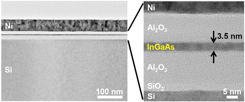
Figure 1: University of Tokyo’s InGaAs on insulator MOSFET.
The US-based SEMATECH industry consortium produced self-aligned III-V MOSFETs on 200mm silicon wafers using standard silicon industry tools for the first time [6.2]. The gate length was 0.5μm (500nm, rather than tens of nanometers used by present-day CMOS). The maximum external transconductance (gm,ext) was 1005μS/μm and the on-current was 1μA/μm at 1V operating voltage. The researchers comment: ‘We present statistically significant data demonstrating that III-V on Si devices can be processed on a Si line with controlled contamination, uniformity and yield while demonstrating good device performance.’
III-V MOSFETs tend to be n-MOS. For CMOS circuitry, one also needs p-MOS. Generally it is expected that these devices will be provided by germanium channels. However, Stanford University, Stanford Linear Accelerator Center, and the Naval Research Lab reported on indium gallium antimonide (InGaSb) devices that had 100% (910cm2/V-s) improved buried mobility for holes, compared with germanium, over the entire sheet charge range [6.4]. The surface mobility was 50% better (620cm2/V-s). The researchers produced transistors with on–off current ratios of 104 with a subthreshold slope (SS) of 120mV/dec. The SS is desired to be as close as possible to the 60mV/dec limit at room temperature (log(10)kT/q) for a sharp turn-on. The devices were produced using aluminum oxide gate insulation in a self-aligned gate-first process.
Quantum well devices are also being developed to incorporate III-Vs into silicon. On the n-side, Pennsylvania State University, Naval Research Lab, and Israel Institute of Technology University have worked with InAs0.8Sb0.2 wells to produce a drive current of 380μA/μm at 0.5V [6.3]. A high-k gate stack consisted of 3.3nm of aluminum oxide and 1nm GaSb, giving an equivalent oxide thickness of 4.2nm. Intel has worked on p-type QWFETs with strained germanium channel and EOT (equivalent oxide thickness) of 1.5nm [6.7]. The hole mobility (770cm2/V-s at sheet carrier density of 5x10¹²/cm2) was found to be 4x that of standard strained silicon. The researchers comment: ‘This suggests the Ge QWFET is a viable p-channel option for III-V CMOS.’
Speedsters
More traditional III-V transistors were also presented, aiming and achieving frequency characteristics up to 1 terahertz (1000GHz = 1THz). Such devices are of interest for millimeter and sub-millimeter radio wave transmissions used for defense and communications, e.g. for signal generation/detection and high-power amplification (GaN or SiC) at high frequency.
The highest characteristic of 1THz was for the maximum oscillation frequency of a 50nm gate-length enhancement-mode In0.7Ga0.3As pseudomorphic HEMT on 100mm InP substrate, produced by Teledyne Scientific (with Jesús del Alamo of MIT) [30.6]. The transconductance was 1.7S/mm at 0.75V 1THz input. A short, thin (10nm) channel was used to maximize carrier transport and minimize contact resistance and parasitic capacitance.
In a related presentation, MIT separately reported on its work with 60nm self-aligned-gate InGaAs HEMTs with cut-off (fT) of 580GHz and maximum oscillation (fmax) of 675GHz [30.7]. This was achieved using a molybdenum-based self-aligned gate that ‘yields outstanding contact resistance, source resistance, transconductance and high-frequency characteristics’.
For GaN HEMT performance, a speed record beyond 400GHz has been achieved by HRL Laboratories with NASA’s Jet Propulsion Laboratory [30.1]. A double heterostructure with barriers above and below the GaN well (AlN/GaN/AlGaN) was used. The gate length was 40nm. The cut-off frequency was 220GHz and the maximum oscillation was 440GHz. Silicon carbide substrates were used. To improve the ohmic contact with the source and drain regions of the device, a re-growth process involving molecular beam epitaxy (MBE) was used.
Further nitride semiconductor HEMT developments were reported by MIT Microsystems Technology Laboratories [30.2], and by University of Notre Dame, TriQuint Semiconductor, and IQE RF LLC [30.4]. The MIT group has developed a gate recess/oxygen plasma treatment to reduce collapse effects in terms of transconductance, enabling an fT of 225GHz. Notre Dame et al produced 144nm gate enhancement-mode and depletion-mode devices on the same wafer, producing ring oscillators with a 15.3psec/stage delay.
GaN nanowires transistors also made a showing, with National Taiwan University presenting a depletion-mode device that operated at 100GHz [30.3]. The channel consisted of the two-dimensional electron gas formed at the interface with a gallium oxide (Ga2O3) nanowire region.
AlGaN/GaN MOS-HEMTs have also been produced for the first time research in Singapore [11.3], by the University of Singapore (NUS), Institute of Materials Research and Engineering, and Data Storage Institute. The device used a diamond-like carbon (DLC) liner with high compressive stress to enhance the performance, increasing saturation currents by up to 30% at 10V (gate at 2V). Peak transconductance was increased by 22% at 5V by using the DLC liner. The gate lengths of the devices were less than 500nm. The researchers believe that the shift of the threshold by 1V in the positive direction suggests the potential of strain engineering for achieving enhancement-mode operation.
High-speed electronics was not exclusively the preserve of III-V devices at IEDM. IHP — Innovations for High Performance Microelectronics (Leibniz-Institut für innovative Mikroelectronik) presented a silicon germanium heterojunction bipolar transistor with fT/fmax of 300GHz/500GHz, a breakdown voltage of 1.6V, and 2psec minimum CML ring oscillator gate delay [30.5]. The researchers attribute these improved results over previous SiGe HBTs to ‘reduced specific collector–base capacitance and base resistance and scaling of device dimensions’.
Light handlers
Another area where III-Vs tend to dominate is light-emitting devices. At IEDM, Dartmouth College and MIT researchers reported on lasers created through band engineering germanium on silicon (both group IV elements). Normally, these group IV materials have indirect bandgaps that make light emission difficult. By compensating the energy difference between the direct and indirect bandgaps, Dartmouth–MIT created laser emission at 1590–1610nm wavelengths using optical pumping (i.e. the energy is delivered into the device through an external light source). However, the researchers also report direct-gap electroluminescence from Ge/Si heterojunction diodes, indicating that electrical pumping is at least possible.
In the light-detection arena, European researcher center IMEC, France’s CRHEA-CNRS, and Royal Observatory of Belgium presented an AlGaN on silicon imager to detect extreme ultraviolet radiation (EUV) [14.5]. The detectors (Figure 2) have a wavelength cut-off of 280nm; the device is thus intrinsically blind to wavelengths longer than this. An array of such detectors was formed into a 256x256-pixel focal plane array with 10μm pixel-to-pixel pitch. The silicon contains 0.35μm CMOS read-out circuitry. The nitride material was deposited using MBE.
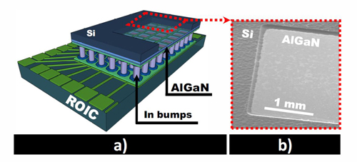
Figure 2: IMEC/CRHEA-CNRS/Royal Observatory of Belgium AlGaN imager after flip-chip integration and Si substrate removal: (a) schematic (not to scale) and (b) top-view SEM of AlGaN membrane.
The structure of the device is such that the illumination comes through the ‘back-side’ – i.e. through the locally thinned silicon wafer. The sensitivity of the device down to 1nm wavelength was verified using synchrotron radiation.
Ultraviolet detection is of particular interest for solar science, EUV microscopy and advanced EUV lithography tools. In fact, the devices were produced within the framework of the BOLD project of the European Space Agency (ESA) [http://bold.sidc.be/-BOLD-GSTP-AlGaN-.htm]. The ultimate aim is to produce 1000x1000-pixel arrays for use on future solar missions.
The use of wide-bandgap nitride semiconductor AlGaN makes the devices more rugged in terms of UV damage compared with devices using silicon. Also, such devices do not need filters to block the visible and infrared radiation that is needed for ‘solar blindness’.
GaN AlGaN SiC HEMT InGaAs FinFET
The author Mike Cooke is a freelance technology journalist who has worked in the semiconductor and advanced technology sectors since 1997.