- News
14 December 2010
Modified p-type layer increases light output from nitride LED
Researchers at Taiwan’s National Cheng-Kung University and National Kaohsiung Marine University have used a selective high barrier region (SHBR) created under the p-electrode of a nitride semiconductor light-emitting diode (LED) to increase light output power by 12% [Ting-Wei Kuo et al, Jpn. J. Appl. Phys., vol49, p116504, 2010].
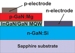 The purpose of the SHBR is to reduce photon absorption in the p-type gallium nitride (p-GaN) hole injection layer and to reduce current crowding under the p-electrode thick metal pad. Current crowding is a particular problem for non-vertical/lateral current flows that are typical in LEDs produced on insulating sapphire substrates. In such cases, both the p- and n-electrodes have to be made from the ‘top’ of the device, and current crowding can occur near the ends of the current path (Figure 1). Localized high charge carrier densities can reduce luminous efficiency in GaN LEDs.
Figure 1: Cross-section sketch of traditional MQW LED on sapphire.
The SHBR was formed by using the inductively coupled plasma (ICP) etch process that is also used to make mesa structures in light-emitting devices and to reach the n-type contact in nitride LEDs produced on insulating sapphire substrates.
The effect of the ICP treatment was first investigated using x-ray photoelectron spectroscopy (XPS) on samples consisting of a magnesium-doped p-type gallium nitride (GaN) layer (0.9μm) on top of undoped GaN (1μm) and sapphire substrate. XPS is performed by measuring the energies of electrons ejected from a material by x-ray illumination.
Two effects were found to result from ICP treatment. First, the Fermi level is moved away from the valence band edge (as reveled by a shift in the Ga 3d spectrum of 0.45eV). The effect of this would be to reduce hole carrier densities. Also, measurements of the nitrogen 1s level suggest that there is an increase in N vacancies in the GaN crystal structure. The Ga/N atomic ratio of the treated samples is found to be 1.42 relative to untreated samples that should have a ratio of 1.
Noise and current/voltage electrical measurements on these samples confirm that the treated GaN becomes highly resistive. Transmission line method measurements give a specific contact resistance of 9.49x10⁻³Ω-cm2 for the untreated GaN, which increases to 5.41x10⁻¹Ω-cm2 for the treated sample.
The researchers used the treatment (in combination with photolithography) to create high-resistance regions in the p-GaN contact of a GaN-based LED. The light-emitting region consisted of a five-period indium gallium nitride (InGaN) multi-quantum well (MQW) structure with GaN barriers. The n-type GaN layer under the MQW was silicon-doped. The layers were grown by metal-organic chemical vapor deposition (MOCVD).
The SHBR was patterned and then an ICP etch was applied using a chlorine (Cl2):boron trichloride (BCl3):argon 10:3:1 mixture. The pressure was 5mTorr and the etch power was 400W with a radio-frequency power of 30W. Comparison devices were also produced without the SHBR. An ICP etch was also used to dig down to the n-GaN layer, forming mesas.
The p-electrodes consisted of nickel-gold (Ni-Au). For the p-electrode a thin layer of Ni-Au (2.5nm/6nm) was deposited first over the p-GaN layer as a transparent conducting layer. Then, thicker layers (15nm/25nm) were used in a smaller area for a pad for wire bonding. The final step was annealing the devices at 400oC in nitrogen for 10mins to create ohmic contacts between the p-GaN and metal layers.
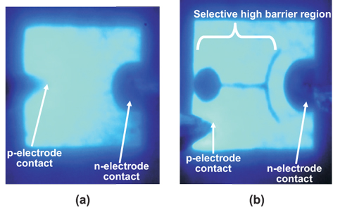
Figure 2: Light emission patterns of LED devices at 1mA forward current without SHBR (a) and with SHBR (b). The locations of n- and p-electrode contacts and the SHBR can also be seen.
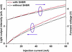 The light intensity (Figure 2) was measured for both devices (Figure 3). While the SHBR device had a higher forward voltage of 3.23V (compared with 3.19V without) at 20mA drive current, the output intensity was increased by 12%. The slight increase in forward voltage is attributed to reduction in the conducting area of the SHBR p-GaN layer. The increased light output is due to an increase in the hole current injected into the active region and a reduction in optical absorption under the electrode, it is suggested.
Figure 3: Comparisons of forward-bias current–voltage and light output–current characteristics of LEDs with and without SHBR.
LEDs GaN InGaN Sapphire substrates MOCVD InGaN/GaN MQW
The author Mike Cooke is a freelance technology journalist who has worked in the semiconductor and advanced technology sectors since 1997.