- News
2 December 2010
Powdec unveils 600V GaN vertical Schottky diode
Powdec K.K. of Oyama City, Japan, which produces gallium nitride (GaN) wafers and devices, has used GaN to develop a Schottky diode with a high breakdown voltage of more than 600V.
 In addition to the vertical Schottky diodes being fabricated on a low-cost, large-diameter sapphire wafer, a proprietary method was developed where the sapphire substate is removed, improving the device's thermal conductance. The GaN diode’s on-resistance is more than 100 times smaller than existing silicon power diodes, reducing power losses by more than 50%, it is reckoned. Powdec plans volume shipments by 2012.
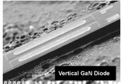
Figure 1: GaN vertical Schottky diode after separation from substrate.
The new GaN Schottky diode can be used in the power conditioning of solar power systems and motor drive circuits, as well as in inverter and power factor correction (PFC) circuits, which are key in the power supply unit of servers and other equipment. Use of the GaN diodes can dramatically lower DC/AC conversion power losses, claims Powdec.
The replacement of existing silicon power diodes by these GaN power diodes can also result in a 15–30% cut in emitted CO2, says the firm. Powdec reckons that its products will enable accelerated adoption of smart grids throughout society (where power and information networks are tied together, and where individually generated electricity from solar power etc can be smoothly connected to the main power grid).
Features of the Schottky diodes include:
- Large-diameter sapphire substrates allow devices to be made at very low cost (as for LEDs).
- At 620V, a leakage current of less than 1mA/cm2 has been achieved. So, for a 10A diode, leakage current will be on the order of 20µA (one-tenth that of other GaN devices).
- The vertical structure does not suffer current collapse, as in lateral devices.
- On-resistance is more than 100 times smaller than that in silicon diodes, providing very low power losses.
- The diode’s thickness is extremely thin at about 20µm (see Figure 2), giving very low conduction resistance and thermal resistance. This enables low power losses and higher operating temperatures as well as reduced system size (since fewer thermal components are needed).
- The GaN Schottky diode provides high-speed performance, so high-frequency operation is possible, allowing a reduction in capacitors and inductors and hence leading to smaller and lower-cost systems.
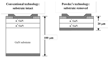
Figure 2: Comparison of device structure using conventional technology and Powdec’s technology.
It has been said in the past that creating a GaN diode with a vertical structure (like a silicon diode) would not be possible unless costly GaN substrates are used, comments Powdec. Sapphire and silicon wafers are lower cost than GaN wafers but, up until now, their use has yielded lower-quality GaN crystal growth on top, reducing the voltage limits of the diode. However, Powdec says that it has developed an innovative epitaxial lateral overgrowth (ELO) technology and realized very high-quality GaN crystal growth on sapphire wafers with dislocation numbers being several hundred times less than that produced by conventional growth technologies, it is claimed.
While Powdec’s new Schottky diode has achieved a breakdown voltage of 620V, the firm says that its proprietary technology also allows the possibility of creating 1200V diodes. Powdec says that it has been granted patents for the technology. The firm adds that, to accelerate market adoption of the low-power GaN devices, it is actively expanding its partnerships worldwide.