- News
24 December 2010
Two-dimensional hole gas with increased density and mobility
The UK’s University of Sheffield and Japanese firm POWDEC KK have developed a technique based on the polarization in nitride semiconductors to create two-dimensional hole gases (2DHGs) with increased carrier density and mobility [Akira Nakajima et al, Appl. Phys. Express, vol3, p121004, 2010].
Two-dimensional electron gases (2DEGs) are the basis for high-electron-mobility transistors (HEMTs). In nitride semiconductors, these 2DEGs arise at the interface between aluminum gallium nitride (AlGaN) and gallium nitride (GaN) due to positive polarization charges. These HEMTs are seen as having potential in power electronics for both high frequencies (cut-off and oscillation frequencies in the hundreds of gigahertz have been achieved) and high voltage (~2000V breakdown was recently reported for one structure).
The Sheffield/POWDEC researchers see possibilities for applying such 2DHGs in creating p-channel heterostructure field-effect transistors (HEMT is the name for n-channel HFETs) and in creating ‘super-junction’ devices that use both 2DHGs and 2DEGs. These possibilities could lead to ultra-low-loss power devices.
Two-dimensional electron gases typically have carrier densities of more than 1013/cm2 and mobilties greater than 1000cm2/V-s. Until now, reported 2DHGs have had densities of less than half this; further, mobility only up to 5cm2/V-s had been observed. These factors combine to give very high sheet resistances for 2DHGs compared with what is obtained with 2DEGs.
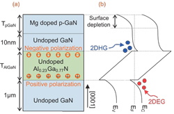 Using simulations of the GaN/AlGaN/GaN double heterostructures (Figure 1), the researchers designed a circular p–n junction diode (Figure 2a) in order to perform C–V measurements. It was expected that both 2DHGs and 2DEGs would be formed. The simulation was used to optimize the thickness of the various layers.
Figure 1: Schematics of (a) layer structure and (b) band diagram.
The structure was grown on sapphire using metal-organic chemical vapor deposition (MOCVD). The top p-GaN (magnesium-doped) layer was 30nm thick. The AlGaN (23% Al) layer was 47nm thick. In normal HEMTs, the AlGaN layer is usually ~20nm thick.
The ohmic contacts of the diode’s anode and cathode were nickel-gold and titanium-aluminum-titanium-gold, respectively. The anode diameter was 600μm.
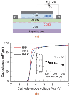 The capacitance (C) of the structure was determined at various bias conditions (V) by using a small 0.1V alternating current modulation at 250kHz. The experiments were carried out at temperatures of 96K, 198K and 298K (Figure 2b). The calculated depletion width of 51–52nm is described as being in good agreements with the AlGaN layer thickness of 47nm determined using x-ray diffraction (XRD).
Figure 2: (a) Simplified schematic of fabricated p–n junction diode. (b) C–V results at different temperatures under reverse bias. Inset: calculated depletion width at zero bias, assuming linear interpolation value of the dielectric constant of AlGaN layer of 8.8ε0.
The C–V measurements suggest the presence of 2DHG and 2DEG either side of the AlGaN layer, as predicted from the group’s simulation (Figure 1). The results are almost temperature independent, so the 2DHG does not freeze out. This behavior is different from that of p-GaN layers where hole carrier densities are strongly temperature dependent due to the high activation energy of the Mg-acceptors.
Hall-effect measurements using the Van der Pauw method at room temperature were carried out on samples with nickel-gold contacts on the p-GaN layer. This gave a sheet resistance of 35kΩ/square, 2DHG carrier density of 1.1x10¹³/cm2, and a hole mobility of 16cm2/V-s.
“This is the first report of experimentally obtained high-density 2DHG over 1013/cm2,” the researchers comment.
The researchers attribute only 9x10¹¹/cm2 of the carrier density to holes arising from the Mg-doping of the 30nm p-GaN layer, an order of magnitude lower than the measured value. Also, the mobility is 10cm2/V-s larger than those of typical Mg-doped layers. The researchers conclude that the majority of holes are induced by polarization charge and not the Mg-doping.
The researchers believe that further improvement of the 2DHG mobility could be achieved through optimization of the layer structure and growth conditions. This is based on a bulk hole mobility of 100cm2/V-s. The degradation to 16cm2/V-s is explained as being due to diffusion of Mg from the p-GaN layer into the undoped GaN beneath.
The work was supported by a variety of UK funding sources under the Newton International Fellowship Scheme of the Royal Society of London, British Academy and Royal Academy of Engineering.
Two-dimensional hole gas AlGaN GaN HEMTs Sapphire substrates
The author Mike Cooke is a freelance technology journalist who has worked in the semiconductor and advanced technology sectors since 1997.