- News
29 December 2010
Improving InGaAsN laser diodes with antimony passivation
Researchers based in Taiwan have developed a passivation technique using antimony (Sb) that improves laser diodes that have indium gallium arsenide nitride (InGaAsN) quantum wells and aluminum gallium arsenide (AlGaAs) optical cladding/confinement [Hsin-Chieh Yu et al, Appl. Phys. Express, vol4, p012103, 2011]. The team contained researchers from National Cheng Kung University, National Taitung University, and Kun Shan University.
InGaAsN quantum wells (with GaAs barriers) provide a simple way to tune emission wavelengths that fall within the 1.3-1.55μm range needed for fiber optic transceiver modules. This is achieved by varying the amount of N incorporation.
Unfortunately, InGaAsN is very sensitive to the presence of aluminum (Al) that is needed to create high refractive index contrasts for optical cladding/confinement in other parts of GaAs-based lasing devices. Effects of Al-containing layers on subsequent InGaAsN material quality include optical deterioration and surface roughness that hamper the development of laser diodes with low threshold currents.
These problems have been seen in both molecular beam epitaxy and in metal-organic chemical vapor deposition. During such processes, Al-containing layers grow on the reaction chamber walls that can decompose and redeposit Al on the epitaxial structure later. Such redeposition seems to be encouraged by the presence of nitrogen in the chamber. Attempts to avoid this situation are complicated, discouraging development of commercial processes.
The epitaxial layers (Table 1) of the various devices were grown using metal-organic chemical vapor deposition. The InGaAsN sources were trimethyl-indium (TMIn), triethyl-gallium (TEGa), tertiarybutylarsine (TBAs), and dimethylhydrazine (DMHy), respectively. For AlGaAs cladding layers, TMAl, TMGa, and arsine (AsH3) were the sources. Zinc and silicon doping for p-type and n-type conduction were provided by DM-zinc (DMZn) and disilane (Si2H6), respectively. The antimonide treatment was supplied by TMSb. High temperature (HT) and low temperature (LT) GaAs layers were grown at 725°C and 510°C, respectively. The TMSb passivation was carried out for 7 minutes at 510°C.
The InGaAsN is used as a quantum well, surrounded by GaAs barriers. Structures with and without AlGaAs cladding were created. One of the AlGaAs samples was subjected to the TMSb treatment before the LT-GaAs layer.
(a) |
(b) |
(c) |
|||
GaAs |
20nm |
GaAs |
20nm |
GaAs |
20nm |
InGaAsN |
7nm |
InGaAsN |
7nm |
InGaAsN |
7nm |
GaAs |
20nm |
GaAs |
20nm |
GaAs |
20nm |
InGaAsN |
7nm |
InGaAsN |
7nm |
InGaAsN |
7nm |
GaAs buffer |
LT GaAs |
20nm |
LT GaAs |
20nm |
|
GaAs substrate |
HT GaAs |
120nm |
TMSb treatment |
||
Al0.3Ga0.7As |
1500nm |
HT GaAs |
120nm |
||
GaAs buffer |
Al0.3Ga0.7As |
1500nm |
|||
GaAs substrate |
GaAs buffer |
||||
GaAs substrate |
|||||
Table 1: Structures of (a) sample Q1: InGaAsN on GaAs, (b) sample Q2: InGaAsN on AlGaAs and (c) sample Q3: InGaAsN on GaAs with TMSb passivation.
Photoluminescence (PL) and atomic force microscopy (AFM) were used to analyze the structures. In the PL studies, the peak emission wavelengths were 1221nm, 1216.5nm and 1213.5nm for the devices without AlGaAs cladding (Q1, Table 1a), with AlGaAs cladding (Q2, Table 1b), and with AlGaAs cladding and TMSb passivation (Q3, Table 1c), respectively. The AlGaAs sample Q2 without TMSb passivation showed a 70% decrease in PL peak intensity compared with Q1. The passivation step giving sample Q3 recovers the intensity lost by Al-contamination in sample Q2. The surface roughness derived from AFM measurements give root mean square values of 0.42nm in Q1, 0.97nm in Q2 (Al cladding), and 0.57nm in Q3 (Al cladding and TMSb passivation). The passivation thus improves the surface morphology over that of the Al cladded sample.
The effect of the Sb is explained as being due to pyrolysis (decomposition of organic material at high temperature in the absence of oxygen) and surfactant effects. The pyrolysis temperature of TMSb is 500°C. The researchers believe this effect of the treatment carries over from the introduction as TMSb up to the deposition of the InGaAsN well, since Sb atoms are not only deposited on the epitaxial structure, but some also stick to the walls of the reactor. The presence of Sb can block residual Al from reacting with the nitrogen sources. Also the surfactant effect of Sb may be continued beyond the treatment layer with effect lasting up to the AlGaAsN layer, improving crystal quality, optical characteristics and surface morphology.
 The amount of TMSb passivation was varied. Higher levels gave increased PL intensity and narrower linewidths. In fact, the Sb treated sample had a narrower linewidth than the sample without Al cladding. Apart from surfactant effects, the researchers suggest that this might be due to Sb incorporation in the GaAs barrier, which forms a strained GaAsSb layer before the highly strained InGaAsN well, improving optical quality and device characteristics.
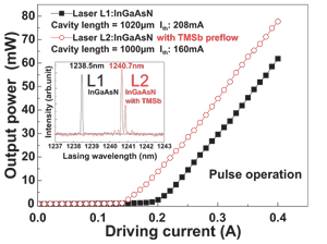
Figure 1: Light output power vs. current curves of InGaAsN single quantum well (SQW) lasers with (L2) and without (L1) TMSb passivation. Inset shows electroluminescence (EL) lasing spectra of the two samples.
Broad area lasers (50μm wide) were produced from the Al cladded materials Q2 and Q3. The cavity lengths were ~1mm. The threshold currents (Figure 1) were, respectively, 208mA and 160mA for the devices without (L1) and with (L2) TMSb passivation. These correspond to densities of 407A/cm2 and 320A/cm2, respectively. The lower threshold current for the passivated device is attributed to better crystal quality. The peak wavelengths were 1238.5nm (L1) and 1240.7nm (L2).
Laser diodes Antimony InGaAsN quantum wells
The author Mike Cooke is a freelance technology journalist who has worked in the semiconductor and advanced technology sectors since 1997.