| Home | About Us | Contribute | Bookstore | Advertising | Subscribe for Free NOW! |
| News Archive | Features | Events | Recruitment | Directory |
News
11 February 2010
Nitride semiconductor illumination through sapphire pyramids
Two different Taiwan research groups have been exploring the use of pyramid-patterned sapphire (pps) substrates to improve nitride semiconductor LED performance. Such substrates have attracted interest as they can give rise to better-quality gallium nitride (GaN) crystal epitaxial growth. A further attraction is an increase in light extraction efficiency in LEDs that emit through the sapphire substrate, since the pyramids reduce total internal reflection effects at the GaN/sapphire interface.
One group, consisting of researchers from the National Central University (NCU) and Academia Sinica, studied the effect of using such substrates on LED output power, achieving a 37% increase over nitride LEDs grown on flat c-plane sapphire [Yi-Ju Chen et al, Jpn. J. Appl. Phys., vol49, p020201, 2010].
The other group, based at the National Chiao Tung University (NCTU), researched the changes in crystal quality and LED performance brought about by changing the slant angle of the pyramids [Ji-Hao Cheng et al, Appl. Phys. Lett., vol96, p051109, 2010].
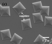 Figure 1:‘Nature-patterned sapphire substrate’ produced by NCU/Academia Sinica. Pyramids measure about 1.5μm laterally and 0.2μm vertically with about 44% average coverage.
The NCU/Academica Sinica group used a maskless
320°C sulfuric acid (H2SO4) wet-etch process to create its pyramids (Figure 1), calling the result a ‘nature-patterned sapphire substrate’ (n-pss). The etch time was for 15, 30 or 60 minutes. The sides of the pyramids were not flat, but rather had dihedral angles of 39° near the base (measured using focused ion-beam techniques), which flattened off to 10° near the apex. The pyramid sides are therefore not crystal planes.
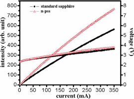 Figure 2: Light output power intensity (L) and voltage (V) vs current (I) for LEDs built using NCU/Academia Sinica n-pss and standard sapphire substrates.
The n-pss substrates were used to create six-period multi-quantum-well indium gallium nitride (InGaN/GaN) LEDs emitting at wavelengths around 450nm (blue). Photoluminescence (PL) measurements gave a higher-intensity signal with a narrower spectral full-width at half maximum (FWHM) compared with standard sapphire. For electroluminescence (EL), the turn-on voltage was about 3.6V at 350mA, similar to the standard LED. However, much greater light output (+37%) was seen for the n-pss LED (Figure 2).
NCTU used a silicon dioxide mask and a ‘hot’ phosphoric acid (H3PO4) wet-etch. The temperature and duration are not mentioned. The pyramids were about 1.2μm high, arranged in a triangular lattice (Figure 3). Four different samples were produced with different slant angle between the c-plane and [101-x] planes. The angle was determined using focused ion-beam and cross-section scanning electron microscopy.
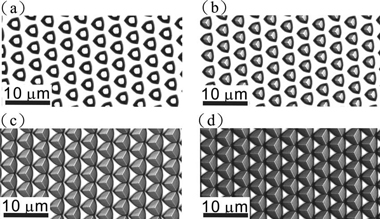
Figure 3: Confocal microscopy images of NCTU PSS: A-PSS (a), B-PSS (b), C-PSS (c), and D-PSS (d).
InGaN/GaN LEDs constructed using these patterned sapphire substrates emitted at a blue wavelength around 448nm on average, at a forward voltage of 3.3V and current of 20mA. The performance of the LEDs (intensity, power, internal quantum efficiency) increased with decreased slant angle (Table 1).
Patterned sapphire substrate |
GaN crystal quality |
LED performance |
|||||||
Etch depth |
c-area ratio |
Slant angle |
x-ray diffraction FWHM (arcsec) |
Etch-pit density |
Average intensity |
Output power |
Internal quantum efficiency |
||
μm |
% |
° |
(002) |
(102) |
x107 /cm2 |
mcd |
mW |
% |
|
A-PSS |
1.20 |
59.6 |
57.4 |
269.3 |
410.3 |
4.31 |
91.2 |
15.2 |
56.5 |
B-PSS |
1.20 |
47.5 |
45.3 |
264.1 |
353.6 |
1.11 |
121.6 |
17.2 |
60.7 |
C-PSS |
1.20 |
21.6 |
38.3 |
251.5 |
312.6 |
0.87 |
131.2 |
18.5 |
61.6 |
D-PSS |
1.20 |
9.6 |
31.6 |
243.4. |
301.2 |
0.52 |
140.0 |
20.8 |
66.1 |
Table 1: Characterizations of NCTU sapphire substrates, GaN crystal layer and LED performance.
Transmission electron microscopy (TEM) and high-resolution TEM (HRTEM) were used to investigate the reasons for the improvement in moving from A to D (Figure 4). Selected-area diffraction (SAD) revealed that the sidewalls of the A pyramids initiated a zincblende GaN crystal structure. The crystal structure of the GaN grown from the flat part of the sapphire (c-plane) was wurtzite. Further characterization of the GaN crystal quality was performed using x-ray diffraction and etching with H3PO4 at 210°C for 2 minutes and determining the density of etch pits (an indication of dislocations).
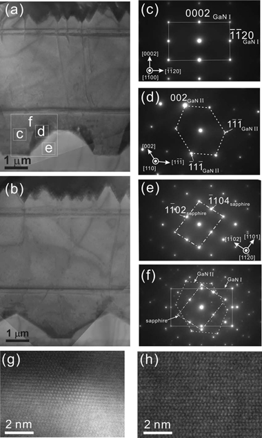
Figure 4: Bright-field TEM images of A-PSS (a) and D-PSS (b). As indicated in (a), SAD patterns showing different crystal structures (c-f). HRTEM images of zincblende structure (GaN II, g) and wurtzite structure (GaN I, h) regions.
The NCTU researchers believe that the improvement in crystal quality for patterned substrates is due to a mechanism similar to that seen in epitaxial lateral over-growth (ELOG), where a silicon dioxide mask is used to block crystal growth from some areas of a GaN substrate. With the patterned sapphire substrates, NCTU believes that the GaN crystal that emanates from the flat c-plane part of the sapphire grows over that coming from the pyramids, creating larger dislocation-free zones of the GaN crystal.
Apart from improved crystal quality resulting from decreased slant angle, the NCTU group performed Monte Carlo simulations of the effect of slant angle on light extraction efficiency through the sapphire substrate (i.e. less reflection back into the GaN LED at the GaN/sapphire interface). The simulations suggested that a smaller slant angle was beneficial also in this respect.
![]() Search: Sapphire substrates GaN LEDs
Search: Sapphire substrates GaN LEDs
Visit: http://jjap.ipap.jp/link?JJAP/49/020201
Visit: http://link.aip.org/link/?APPLAB/96/051109/1
The author Mike Cooke is a freelance technology journalist who has worked in the semiconductor and advanced technology sectors since 1997.
![]() ©2010 Juno Publishing and Media Solutions Ltd. All rights reserved. Semiconductor Today and the editorial material contained within it and related media is the copyright of Juno Publishing and Media Solutions Ltd. Reproduction in whole or part without permission from Juno Publishing and Media Solutions Ltd is forbidden. In most cases, permission will be granted, if the author, magazine and publisher are acknowledged.
©2010 Juno Publishing and Media Solutions Ltd. All rights reserved. Semiconductor Today and the editorial material contained within it and related media is the copyright of Juno Publishing and Media Solutions Ltd. Reproduction in whole or part without permission from Juno Publishing and Media Solutions Ltd is forbidden. In most cases, permission will be granted, if the author, magazine and publisher are acknowledged.
Disclaimer: Material published within Semiconductor Today and related media does not necessarily reflect the views of the publisher or staff. Juno Publishing and Media Solutions Ltd and its staff accept no responsibility for opinions expressed, editorial errors and damage/injury to property or persons as a result of material published.
Semiconductor Today, Juno Publishing and Media Solutions Ltd, Suite no. 133, 20 Winchcombe Street, Cheltenham, GL52 2LY, UK
Web site by No Name No Slogan ![]()