| Home | About Us | Contribute | Bookstore | Advertising | Subscribe for Free NOW! |
| News Archive | Features | Events | Recruitment | Directory |
News
28 January 2010
Gate control of terahertz transistor emission frequency
Researchers, based in Europe and Japan, have demonstrated terahertz (THz) electromagnetic radiation from high-electron-mobility transistors (HEMT) whose emission frequency peaks are tunable by the gate voltage [El Fatimy et al, J. Appl. Phys., vol107, p024504, 2010].
Field-effect transistors (FETs) have been known to emit THz and sub-THz wave since the 1980s. This radiation is thought to arise from plasma waves in the device either from heating of the electrons by the external field or from instabilities of the electron flow due to plasma wave amplification from reflections at device boundaries.
It has been expected that the plasma wave frequency characteristics should be tunable by the gate voltage, although previously this has only been shown in the detection of THz radiation by FETs. Among the mechanisms possibly obscuring tunable emission, hot plasmon or edge plasma wave instabilities with wide spectral characteristics have been proposed.
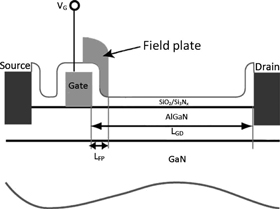 Figure 1: HEMT with gate covered by a field plate.
The latest research uses aluminum gallium nitride on gallium nitride (AlGaN/GaN) HEMTs (Figure 1) grown by metal-organic chemical vapor deposition (MOCVD). A 4H silicon carbide (SiC) substrate was used. The gate structure was T-shaped with dimensions 2x50μm and 2x100μm, giving two different samples (1 and 2, respectively — see Table 1). The ohmic source–drain contacts were Ti/Al/Ni/Au layers and the gate metal stack consisted of Ni/Au.
Table 1: Physical characteristics of HEMTs used in study. Vth = threshold voltage.
Sample |
1 |
2 |
|
Gate width |
μm |
2x50 |
2x100 |
Gate length |
nm |
150 |
250 |
Vth |
V |
–5.1 |
–4.8 |
Field plate? |
no |
yes |
The emissions came from square source–drain pulses with a 30Hz frequency and a 0.5 duty cycle at room temperature. The registration of the radiation was performed by a silicon bolometer at 4K with spectral analysis performed by a Fourier transform spectrometer under vacuum. The frequency range of the bolometer was 0.2–4.5THz. The results were normalized according to a reference spectrum from the HEMT in the spectrometer’s vacuum chamber with no applied voltage. The spectra therefore reflect the relative increase in emission from the HEMT.
The researchers report that they had improved their experimental configuration compared with their previous work, allowing a narrowing of spectral resolution from wave numbers of 15/cm to 1/cm.
It is found that the THz emission appears in a threshold-like manner, depending on the drain–source bias (Vds). Increasing the negative gate bias pushes the onset of emission to lower Vds. The frequency shift with gate voltage for the longer-gate device accords well with theoretical expectations that the emission results from the excitation of plasma waves (Figure 2, solid line). The prediction for the shorter device (with different ‘effective gate length’ and ‘gate-to-channel voltage swing’) is only followed ‘in a qualitative way’ in the sense that the frequencies are higher for the shorter-gate sample and decrease somewhat for increasing negative gate bias. The predictions are based on the behavior of the fundamental frequency of the plasma waves in the device.
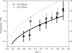 Figure 2: Position of emission spectrum peak as function of gate bias for HEMTs with 150nm and 250nm gate lengths at Vds = 4V. The lines (solid line, 250nm gate; dotted, 150nm) correspond to calculations based plasma wave fundamental frequency dependence.
The gate dependence of the emission line-widths is also seen as confirmation of this theoretical mechanism. The line-width depends on damping of the plasma waves and hence on the mobility. The mobility degrades with increasing carrier density in the channel. At low negative gate bias (~0V), the full-width at half maximum (FWHM) is about 2.5THz. This reduces to around 1.6THz at –3.5V where the carrier density is reduced (increasing the mobility).
“We estimate that the observed spectrum broadening corresponds to the mobility degradation from 1700 to 1100cm2/V-s, which are quite reasonable values for our samples,” the researchers comment.
The corresponding author of the paper, Abdel El Fatimy, is based at the universities of Tohoku (Japan) and Cardiff (Wales, UK). Along with another researcher from Tohoku, the work involved scientists from the universities of Montpellier (France) and Salamanca (Spain), Institut d’Electronique et de Microélectronique du Nord (France), Thales Research and Technology (France) and Institute of High Pressure Physics (UNIPRESS, Poland).
![]() Search: Terahertz radiation AlGaN/GaN HEMTs MOCVD SiC substrates
Search: Terahertz radiation AlGaN/GaN HEMTs MOCVD SiC substrates
Visit: http://link.aip.org/link/?JAPIAU/107/024504/1
The author Mike Cooke is a freelance technology journalist who has worked in the semiconductor and advanced technology sectors since 1997.
![]() ©2010 Juno Publishing and Media Solutions Ltd. All rights reserved. Semiconductor Today and the editorial material contained within it and related media is the copyright of Juno Publishing and Media Solutions Ltd. Reproduction in whole or part without permission from Juno Publishing and Media Solutions Ltd is forbidden. In most cases, permission will be granted, if the author, magazine and publisher are acknowledged.
©2010 Juno Publishing and Media Solutions Ltd. All rights reserved. Semiconductor Today and the editorial material contained within it and related media is the copyright of Juno Publishing and Media Solutions Ltd. Reproduction in whole or part without permission from Juno Publishing and Media Solutions Ltd is forbidden. In most cases, permission will be granted, if the author, magazine and publisher are acknowledged.
Disclaimer: Material published within Semiconductor Today and related media does not necessarily reflect the views of the publisher or staff. Juno Publishing and Media Solutions Ltd and its staff accept no responsibility for opinions expressed, editorial errors and damage/injury to property or persons as a result of material published.
Semiconductor Today, Juno Publishing and Media Solutions Ltd, Suite no. 133, 20 Winchcombe Street, Cheltenham, GL52 2LY, UK
Web site by No Name No Slogan ![]()