| Home | About Us | Contribute | Bookstore | Advertising | Subscribe for Free NOW! |
| News Archive | Features | Events | Recruitment | Directory |
News
25 January 2010
SEI explains polarization clues to optimal GaN green laser stripes
Japan’s Sumitomo Electric Industries (SEI) has been studying optical polarization of light emitted from green laser diode (LD) structures as a guide to the optimal construction of laser stripes [Takashi Kyono et al, Appl. Phys. Express, vol3, p011003, 2010].
SEI has registered recent successes in using gallium nitride (GaN) substrates with the semi-polar {20-21} surface plane to create LDs with 531nm true green (520–570nm) pulsed laser emission as well as continuous wave (cw) operation at 520nm. SEI produces these substrates using hydride vapor phase epitaxy (HVPE).
By using these substrates, the researchers have been able to grow high indium (In) content quantum well (QW) layers with high quality to access the longer green wavelengths, compared with lasers that emit in the near-ultraviolet to blue wavelength ranges (375–470nm) using nitride semiconductors with various combinations of aluminum (Al), indium and gallium.
The effect of using semi-polar substrates is to reduce the internal electric fields arising spontaneously and when the material is strained (piezoelectricity). This results in smaller blue-shifts between the non-lasing and lasing states.
In the latest research, SEI researchers have studied the polarization ratio dependence under electroluminescence (EL) with peak wavelength and current density to help determine the best laser strip orientation on {20-21} substrates.
The LD structure consists of a series of layers grown using metal-organic chemical vapor deposition (MOCVD): n-type GaN buffer, n-type InAlGaN cladding, n-type InGaN waveguide, multiple QW (MQW) active region (3x 3nm InGaN wells, 2x GaN barriers), p-type AlGaN electron blocker, p-type InGaN waveguide, p-type InAlGaN cladding, and p-type GaN contact. The same structure — without the cladding and waveguides — has also been used for light-emitting diode (LED) structures. The aim of the LED structures was to see the effect of strain on polarization.
 Both epitaxial wafer structures were processed into surface-emitting structures for pulsed EL measurements. A semi-transparent p-type electrode was used on the surface, while an n-type electrode was deposited on the back-side of the wafer.
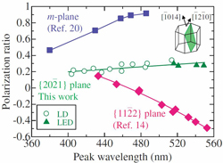
Figure 1 (above): Polarization ratio vs peak wavelength under a current density of 7.4A/cm2, compared with results of other groups using m-plane MQWs with 3nm wells (Rohm, phospholuminescence) and {11-22} plane 3.1nm single QWs (UCSB/Mitsubishi, EL with current density 10A/cm2).
The polarization ratio shows a small increase as the peak wavelength increases (Figure 1). In fact, a higher polarization ratio would be advantageous for lasing and it was found that miscutting the substrate in the m-plane direction increased it to 0.49 at 513nm with a +4° angle and decreased it to 0.12 with a -4° angle at 516nm. The researchers were somewhat surprised by this result, since previously reported theoretical calculations had suggested only a slight effect from such miscutting.
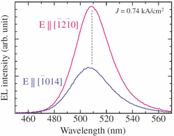 Figure 2: Polarized EL spectra of green LED on {20-21} plane GaN substrate at 0.74kA/cm2 current density.
Also, the polarization for the non-miscut LDs with current density was almost constant up to 0.74kA/cm2. In addition, the stronger polarization component was found to have a slightly longer wavelength (Figure 2). This is interpreted as being due to the stronger component resulting from an optical transition between the conduction band and the highest valence band (lower photon energy and hence longer wavelength).
Another interesting observation is that the LED structures are on the same trend line as the LD structures. Researchers at University of California Santa Barbara and Rohm found a shift towards positive polarization values for {11-22} plane LDs over comparable LEDs due to strain relaxation from defect introduction. The SEI researchers suggest their use of lattice-matched InAlGaN cladding was responsible for the suppression of strain relaxation effects that can modify electronic band structures.
The SEI researchers conclude from their work that a laser stripe along the [-1014] direction is to be preferred over a [-12-10] direction. To confirm this, they constructed LDs with these stripe directions. The threshold current with [-1014] stripes was a quarter that of [-12-10] stripes. In addition, [-1014] stripes lased at a longer wavelength: 512nm rather than 503nm. This wavelength increase is not due solely to the wavelength difference between the polarization components, but is due rather to the lower threshold voltage, meaning that there is a lower blue-shift in going from spontaneous to stimulated emission.
“Based on these analyses, we have adopted such device designs for our green LDs and have achieved 520-531nm lasing, as reported in detail in the previous studies,” the researchers comment.
See related items:
Sumitomo boosts 520nm green InGaN laser to continuous-wave operation
Sumitomo Electric claims first pure-green semiconductor laser
Nichia pushes InGaN lasers nearer to green via 515nm emission
Osram Opto claims first 500nm InGaN laser
![]() Search: Sumitomo Electric Green laser diode GaN
Search: Sumitomo Electric Green laser diode GaN
Visit: http://apex.ipap.jp/link?APEX/3/011003
Visit: http://global-sei.com

![]() ©2010 Juno Publishing and Media Solutions Ltd. All rights reserved. Semiconductor Today and the editorial material contained within it and related media is the copyright of Juno Publishing and Media Solutions Ltd. Reproduction in whole or part without permission from Juno Publishing and Media Solutions Ltd is forbidden. In most cases, permission will be granted, if the author, magazine and publisher are acknowledged.
©2010 Juno Publishing and Media Solutions Ltd. All rights reserved. Semiconductor Today and the editorial material contained within it and related media is the copyright of Juno Publishing and Media Solutions Ltd. Reproduction in whole or part without permission from Juno Publishing and Media Solutions Ltd is forbidden. In most cases, permission will be granted, if the author, magazine and publisher are acknowledged.
Disclaimer: Material published within Semiconductor Today and related media does not necessarily reflect the views of the publisher or staff. Juno Publishing and Media Solutions Ltd and its staff accept no responsibility for opinions expressed, editorial errors and damage/injury to property or persons as a result of material published.
Semiconductor Today, Juno Publishing and Media Solutions Ltd, Suite no. 133, 20 Winchcombe Street, Cheltenham, GL52 2LY, UK
Web site by No Name No Slogan ![]()