| Home | About Us | Contribute | Bookstore | Advertising | Subscribe for Free NOW! |
| News Archive | Features | Events | Recruitment | Directory |
News
20 July 2010
Quantum wells with AlGaN barriers increases blue-green laser light output
Researchers from the University of California Santa Barbara (UCSB) have reported improved 516nm ‘green’ laser diode performance from using aluminum gallium nitride (AlGaN) for the quantum well barriers [You-Da Lin et al, Appl. Phys. Express, vol3, p082001, 2010].
Normally, gallium nitride (GaN) or indium gallium nitride (InGaN) is used for quantum well barriers. AlGaN generally has a wider bandgap energy than either of these alternatives. It is widely used for electron-blocking layers in light-emitting diodes and laser diodes to reduce unwanted recombination in the p-type contact region. UCSB’s wells used traditional InGaN material with narrower bandgap energies.
Much research work has recently been directed to producing green lasers with wavelengths longer than 520nm – the UCSB device is therefore more strictly ‘blue-green’. The aim of this work is to produce projector systems that produce the red, green and blue light directly from laser diodes. Presently in commercial projector systems, the red and blue light comes from laser diodes, but the green component is produced from infrared lasers using frequency-doubling arrangements. This is complex, costly and less compact than desired.
Although c-plane nitride semiconductor laser diodes have reached 532nm under pulsed operation, the wall-plug efficiency is low. One factor hindering the performance of such devices is the high polarization fields in the c-plane direction in nitride semiconductors that tend to pull the electrons and holes apart, reducing their ability to recombine as light. UCSB has been among those research groups that have looked to laser devices grown in alternative crystal directions to reduce or eliminate this ‘quantum confined Stark effect’ (QCSE).
So far, the wavelengths of these devices have been restricted to less than 500nm, largely because it is difficult to grow high-quality material. Growing InGaN wells is particularly hard – indium incorporation tends to create non-uniform regions of high and low concentrations (indium segregation), and basal stacking plane faults are easy to create in non-polar m-plane grown devices.
UCSB has tried semi-polar growth directions using free-standing GaN material supplied by Mitsubishi. In its latest work it has used (20-21) substrates. Last year, Sumitomo reported such (20-21) devices that emitted 531nm-wavelength light under pulsed operation, and UCSB spin-off Kaai Inc reported continuous-wave devices emitting at 523nm earlier this year at the SPIE conference.
The new research from UCSB compared devices with GaN (laser A), Al0.05Ga0.95N (B) and In0.03Ga0.97N (C) barriers. The active region consisted of three-period quantum wells with 4.5nm InGaN wells and 10nm barriers. The EBL consisted of 10nm of Al0.2Ga0.8N. The n-contact consisted of 1μm of silicon-doped GaN grown before the cladding, waveguide and active layers. The p-contact was 100nm Mg-doped GaN grown after the EBL, waveguide and cladding. The cladding and waveguide layers were doped GaN and InGaN, respectively. The laser cavities were 2μm x 1200μm ridges with the end facets cleaved and coated with distributed Bragg reflectors of successive layers of silicon dioxide and tantalum pentoxide. The reflectivities for the front and rear facets were 97% and 99%, respectively.
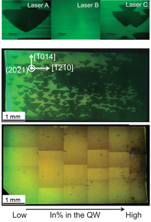 Figure 1. Fluorescence micrographs of small regions of laser material A, B and C (top) and for whole epiwafer (middle, laser A; bottom, laser B). The increase in photoluminescence wavelength from left to right is unintentional. The increase indicates higher indium content in the alloy.
Inspection of the material under optical and fluorescence microscopes showed ~100μm non-luminescent triangular regions which were attributed to defects that presumably would give rise to non-radiative recombination and hence low output power for laser diodes. The material for lasers A and C showed large triangles, while that for the laser B material using AlGaN barriers shows uniform QW emission without non-luminescent regions (Figure 1). A wider-field inspection on the wafer-level did find some small triangular regions in the B sample. In fact, the wafers were non-uniform in the density of triangular regions, which is an effect attributed to non-uniformity in the growth process temperature.
The electroluminescence (EL) spontaneous emission peak wavelength for laser B was well within the green region at 527nm. The AlGaN barrier increased the EL of the devices significantly compared with those made of GaN or InGaN. The UCSB researchers believe that the use of AlGaN barriers “provides a pathway to high internal quantum efficiency in the green and yellow spectrum regions.”
The researchers tested the lasing properties under pulsed operation with a 0.01% duty cycle (Figure 2). Sample device B had a threshold of 720mA that corresponded to a current density of 30kA/cm2. Spontaneous emission at a driving current of 20mA showed a peak at 528nm; this blue-shifted to 516nm above laser threshold.
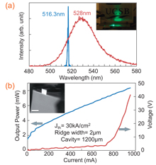 Figure 2. (a) Representative spectra of spontaneous emission with drive current of 20mA and 516nm stimulated emission with drive current above threshold of the laser with AlGaN barriers. Inset: far-field pattern of 516nm laser diode. (b) Light output power–current–voltage (L–I–V) curves of LDs under pulsed operation (duty cycle = 0.01%). Inset: representative scanning electron microscope image of cleaved facet.
Based on simulation work, the researchers believe that optical confinement could be improved by increasing the indium content in the guiding layers and by reducing the aluminum content in the barriers. However, the minimum Al composition in the AlGaN barrier that is needed in order to improve the emission uniformity and internal efficiency is 3%.
One of the researchers involved in the UCSB research is also of Sharp Corp, and another came from Mitsubishi Chemical Corp.
![]() See related items:
See related items:
Nichia to ship sample green laser diodes from August
Yet another angle on nitride laser diodes
Search: Green laser diodes GaN InGaN
Visit: http://apex.ipap.jp/link?APEX/3/082001
Visit: www.kaai.com
The author Mike Cooke is a freelance technology journalist who has worked in the semiconductor and advanced technology sectors since 1997.
![]() ©2010 Juno Publishing and Media Solutions Ltd. All rights reserved. Semiconductor Today and the editorial material contained within it and related media is the copyright of Juno Publishing and Media Solutions Ltd. Reproduction in whole or part without permission from Juno Publishing and Media Solutions Ltd is forbidden. In most cases, permission will be granted, if the author, magazine and publisher are acknowledged.
©2010 Juno Publishing and Media Solutions Ltd. All rights reserved. Semiconductor Today and the editorial material contained within it and related media is the copyright of Juno Publishing and Media Solutions Ltd. Reproduction in whole or part without permission from Juno Publishing and Media Solutions Ltd is forbidden. In most cases, permission will be granted, if the author, magazine and publisher are acknowledged.
Disclaimer: Material published within Semiconductor Today and related media does not necessarily reflect the views of the publisher or staff. Juno Publishing and Media Solutions Ltd and its staff accept no responsibility for opinions expressed, editorial errors and damage/injury to property or persons as a result of material published.
Semiconductor Today, Juno Publishing and Media Solutions Ltd, Suite no. 133, 20 Winchcombe Street, Cheltenham, GL52 2LY, UK
Web site by No Name No Slogan ![]()