| Home | About Us | Contribute | Bookstore | Advertising | Subscribe for Free NOW! |
| News Archive | Features | Events | Recruitment | Directory |
News
5 July 2010
Demonstrating phosphide–nitride semiconductor integration with silicon
Researchers at Toyohashi University of Technology in Japan have developed gallium phosphide nitride (GaPN) light-emitting devices as part of a monolithic optoelectronic integrated circuit including silicon MOSFETs [Keisuke Yamane et al, Appl. Phys. Express, vol3, p074201, 2010].
These devices are seen as a possible route to miniaturization of electronics that could provide an alternative to the increasingly difficult scaling of the silicon CMOS logic that powers most consumer electronics. The present silicon CMOS scale is of the order of tens of nanometers. Intel began marketing processors with 32nm technology earlier this year.
Although integration of light-emitting devices (LEDs and lasers) with silicon has been attempted by a number of groups, less attention has been paid to the possibility of integrating these devices with silicon circuitry.
One problem in the path of integrating light-emitting compound semiconductors with silicon has been the lattice mismatches between the respective materials that lead to crystal imperfections and hence to reduced performance of the resulting devices.
Defects at the interface between silicon substrates and gallium phosphide (GaP) have been reduced by migration-enhanced epitaxy (MEE), where the sources are pulsed to allow stable surfaces to form. However, an alternative route is to reduce or eliminate the lattice mismatch by introducing a new parameter through creating alloys such as between GaP and gallium nitride (GaN).
The Toyohashi group has previously proposed the use of III-V-N compound semiconductors for integration with silicon, creating indium gallium phosphide nitride (InGaPN)/GaPN double-heterostructure and gallium arsenide nitride (GaAsN)/GaPN quantum well structures. In addition, the group has developed MOSFETs on the silicon layers used to cap the compound semiconductor layers.
The researchers now report the successful creation of a bit-counter circuit with an optical output (Figure 1). A dual-chamber molecular beam epitaxy (MBE) system was used to grow the n-Si/p-GaPN/n-GAPN/GaP/n-Si heterostructure. The n-Si (100) substrate was misoriented by 4° towards the [011] direction. The thin 20nm GaP layer was grown using MEE after thermal treatment of the substrate. The incorporation of this thin layer is found to ‘significantly’ decrease structural defects in subsequent layers such as antiphase domains, threading dislocations, and stacking faults. The n-GaPN layer was 500μm and the p-GaPN 600μm. The carrier concentrations in these layers were found to be 5x10¹⁷/cm3.
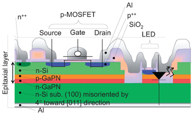
Figure 1: Schematic cross section of part of the 1-bit counter IC consisting of p-MOSFET and LED.
The silicon capping layer was first grown at the same temperature as the GaPN layers (550°C) for 100nm and then 1.4μm was deposited at 850°C. The aim of this was to reduce the incorporation of P atoms in the capping layer. The use of a dual-chamber system also reduces this effect (Table 1), reducing the carrier concentrations in the capping layer. This reduction in n-type concentrations enables a reduction in the threshold voltage and increases the channel mobility in the silicon MOSFETs produced. The 850°C growth was also found not to affect the abruptness of the interfaces between the compound semiconductor layers and the n-Si substrate and capping layer. The group believes that further investigation of the P incorporation using secondary-ion mass spectrometry (SIMS) is needed to fully explain the residual carrier concentrations in the Si cap.
Growth system |
Temperature |
Carrier concentration |
Threshold voltage |
Channel mobility |
° C |
1017/cm3 |
V |
cm2/V-s |
|
Single chamber |
590 |
30–67 |
— |
— |
Dual chamber |
590 |
4.4–6.6 |
—3.1 |
58 |
Dual chamber |
850 |
0.8–1.2 |
—2.1 |
82 |
Table 1: Carrier concentration of Si-capping layers grown using single- and dual-chamber MBE systems and threshold voltage and channel mobility of p-MOSFETs. The conditions used and properties resulting in the present work are indicated in the last row.
The bit-counter circuit with optical output was then created using this material (Figure 2). The circuit contained enhancement–enhancement inverters (5x parallel drive p-MOSFETs, 1x load p-MOSFET) and p-MOSFET switches, along with input and output indicator LEDs. The fabricated p-MOSFETs had 7μm gate length and 30μm gate width. The LEDs measured 100μm x 100μm and were driven using 16 parallel p-MOSFETs (50μm width). The wiring was done in a single layer of aluminum for simplicity. The output LED fired after two input pulses.
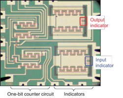 Figure 2: Micrograph of fabricated chip with one-bit counter circuit with optical output.
The red light from the LEDs was in step with the voltage levels in the circuit. However, there was also some light emission from the p-MOSFET regions, which was determined to be due to reverse bias being applied at the n-Si/p-GaPN heterojunction at certain points of the operation of the device. The operating voltage of the device was relatively high and the reverse bias caused a relatively large leakage current into the GaPN, causing light emission there. The researchers believe that this effect can be mitigated by reducing the operating voltage through optimization of the doping and the Si cap thickness in the LED region.
Visit: http://apex.ipap.jp
The author Mike Cooke is a freelance technology journalist who has worked in the semiconductor and advanced technology sectors since 1997.
![]() ©2010 Juno Publishing and Media Solutions Ltd. All rights reserved. Semiconductor Today and the editorial material contained within it and related media is the copyright of Juno Publishing and Media Solutions Ltd. Reproduction in whole or part without permission from Juno Publishing and Media Solutions Ltd is forbidden. In most cases, permission will be granted, if the author, magazine and publisher are acknowledged.
©2010 Juno Publishing and Media Solutions Ltd. All rights reserved. Semiconductor Today and the editorial material contained within it and related media is the copyright of Juno Publishing and Media Solutions Ltd. Reproduction in whole or part without permission from Juno Publishing and Media Solutions Ltd is forbidden. In most cases, permission will be granted, if the author, magazine and publisher are acknowledged.
Disclaimer: Material published within Semiconductor Today and related media does not necessarily reflect the views of the publisher or staff. Juno Publishing and Media Solutions Ltd and its staff accept no responsibility for opinions expressed, editorial errors and damage/injury to property or persons as a result of material published.
Semiconductor Today, Juno Publishing and Media Solutions Ltd, Suite no. 133, 20 Winchcombe Street, Cheltenham, GL52 2LY, UK
Web site by No Name No Slogan ![]()