| Home | About Us | Contribute | Bookstore | Advertising | Subscribe for Free NOW! |
| News Archive | Features | Events | Recruitment | Directory |
News
9 June 2010
InAlN provides better electron-blocking layer in nitride LEDs
Indium aluminum nitride (InAlN) electron-blocking layers (EBLs) may lead to more efficient nitride semiconductor light-emitting diodes (LEDs) and be better at tackling ‘droop’ effects than traditional aluminum gallium nitride (AlGaN), according to research by Georgia Institute of Technology and Arizona State University (ASU) [Suk Choi, Appl. Phys. Lett., vol96, p221105, 2010].
Designers of LED structures use EBLs to attempt to confine the recombination of electron–hole charge carriers to the active region where light emission is (or should be) the most likely result. Recombination outside the active region is more likely to be non-radiative. Any radiation from such recombination will also be outside of the designed wavelength/frequency of the device.
Electrons are more mobile and hence more likely to overshoot the active region and end up recombining in the p-type contact – hole-blocking layers are rarely employed. AlGaN is normally used in EBLs because it has a wider energy bandgap than the GaN barriers and InGaN wells in the active region.
One problem is that strain effects from lattice mismatches between the EBL and active layers can create strain-based piezoelectric fields in the active region. Further problems arise from the different spontaneous polarization fields. These fields act in a sense that reduces the barrier’s effectiveness. Adding more Al to the AlGaN to increase the bandgap, also increases these polarization field effects. It is also difficult to grow good-quality high-Al-content AlGaN layers.
The optimum growth temperature for AlGaN can also be quite high, producing significant damage in the underlying layers, particularly for the high-In-content InGaN (>20%) that is needed for longer-wavelength devices.
InAlN has recently been developed as a barrier in high-electron-mobility transistors (see Reducing GaN HEMT degradation with InAlN barrier and Pushing AlInN and AlGaN HEMTs further on SiC and silicon), as cladding in laser diodes, and as a low-refractive-index component of distributed Bragg reflectors.
In March, Georgia Tech/ASU reported the use of InAlN as an EBL [Hee Jin Kim et al, Appl. Phys. Lett., vol96, p101102, 2010]. Among the material’s attractive features is that it can be lattice matched to GaN and InGaN, reducing piezoelectric effects. In addition to having a wide energy bandgap, InAlN also has a large conduction-band offset relative to GaN (presenting a large barrier to electrons entering the p-type region) and relatively small valence-band offset (so that holes can get into the active region).
Growth of InAlN also takes place at a lower temperature than AlGaN, leading to less damage to the active region. However, researchers developing InAlN have had difficult challenges to overcome, arising from the very different optimal growth temperatures and pressures for InN and AlN.
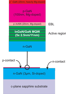 Now Georgia Tech/ASU have carried out comparisons with blue LEDs containing either AlGaN or InAlN EBLs, along with devices with no EBL. Metal-organic chemical vapor deposition was used to grow the devices (Figure 1, top). The InAlN contained 18% In and was grown at 845°C. The AlGaN contained 20% Al and was grown at 930°C. In the non-EBL devices, the layer was replaced with 20nm of p-GaN.
Figure 1: Schematic of LEDs grown by Georgia Tech/ASU to show effectiveness of InAlN as electron-blocking layer compared with AlGaN EBL or no EBL.
Standard top-emitting LEDs were produced from the epitaxial material with mesa structures, and n- and p-contacts consisting of titanium-aluminum-titanium-gold and nickel oxide-gold, respectively (Figure 1, bottom).
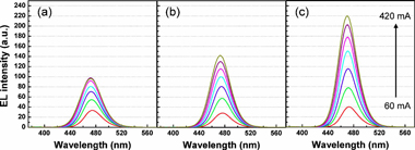
Figure 2 (above): Electroluminescence (EL) spectra from Georgia Tech/ASU LEDs without EBL (a), with AlGaN EBL (b), and with InAlN EBL (c). Injection current was applied in pulsed mode (10ms, 10% duty cycle).
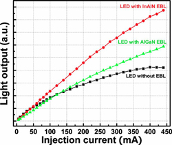 Figure 3 (right): Light output versus current (L-I) characteristics of LEDs.
The peak emission wavelengths at 60mA were 475nm, 476nm and 473nm for non-EBL, AlGaN EBL and InAlN EBL devices, respectively (Figure 2). The peak intensities went (from lowest to highest) non-EBL, AlGaN EBL, and InAlN EBL. At lower current injection (<40mA), the non-EBL device does produce more light than those with EBLs. This is seen as being due to the absence of a barrier to hole injection into the active region in these devices. However, the quantum efficiency (integrated electroluminescence intensity/injection current) of the non-EBL device droops rapidly at higher currents, leading to a sub-linear saturation of the light output at higher current (Figure 3).
In fact all the devices show the droop effect, which is commonly seen in InGaN-based LEDs. However, the current at which the droop sets in, and the speed of descent, are different for the various devices. Without an EBL, the droop sets in at an injection current density of 3A/cm2. The respective current densities for the AlGaN and InAlN EBL devices are 6A/cm2 and 11.5A/cm2.
The speed of the droop was indicated by the size of the drop in quantum efficiency from the peak value to that at 360A/cm2 injection current density. For the non-EBL device the drop was 69%, for the AlGaN device 32%, and for the InAlN device only 18%.
Another advantage of the InAlN EBL device is that it has a peak efficiency that is intermediate between the AlGaN EBL and non-EBL devices, enabling it to produce more light than either of its competitors at higher currents.
The most popular theory of why the droop occurs is a form of Auger recombination, but there are supporters of other mechanisms such as limited hole transport into the active region, polarization effects, a combination of effects, etc.
The work was carried out with US Department of Energy funding, along with support from SAFC Hitech, financial backing from Japanese nitride-based LED maker Nichia, and the Georgia Research Alliance.
See related items:
Pushing AlInN and AlGaN HEMTs further on SiC and silicon
Reducing GaN HEMT degradation with InAlN barrier
![]() Search: InAlN EBLs LEDs Droop effect
Search: InAlN EBLs LEDs Droop effect
Visit: http://link.aip.org
The author Mike Cooke is a freelance technology journalist who has worked in the semiconductor and advanced technology sectors since 1997.
![]() ©2010 Juno Publishing and Media Solutions Ltd. All rights reserved. Semiconductor Today and the editorial material contained within it and related media is the copyright of Juno Publishing and Media Solutions Ltd. Reproduction in whole or part without permission from Juno Publishing and Media Solutions Ltd is forbidden. In most cases, permission will be granted, if the author, magazine and publisher are acknowledged.
©2010 Juno Publishing and Media Solutions Ltd. All rights reserved. Semiconductor Today and the editorial material contained within it and related media is the copyright of Juno Publishing and Media Solutions Ltd. Reproduction in whole or part without permission from Juno Publishing and Media Solutions Ltd is forbidden. In most cases, permission will be granted, if the author, magazine and publisher are acknowledged.
Disclaimer: Material published within Semiconductor Today and related media does not necessarily reflect the views of the publisher or staff. Juno Publishing and Media Solutions Ltd and its staff accept no responsibility for opinions expressed, editorial errors and damage/injury to property or persons as a result of material published.
Semiconductor Today, Juno Publishing and Media Solutions Ltd, Suite no. 133, 20 Winchcombe Street, Cheltenham, GL52 2LY, UK
Web site by No Name No Slogan ![]()