| Home | About Us | Contribute | Bookstore | Advertising | Subscribe for Free NOW! |
| News Archive | Features | Events | Recruitment | Directory |
News
21 June 2010
Solar nanowire research targets 65% efficiency
Researchers at Technische Universiteit Eindhoven (TU/e), Philips and Philips’ MiPlaza research service company hope to achieve 65% efficient solar cells using semiconductor nanowire technology with €1.2m funding from the Dutch government. By placing the devices in southern Europe and North Africa and using mirror concentrator systems (Figure 1), it is believed that such devices could generate a substantial portion of Europe’s electricity demand.
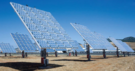 Figure 1: Concentrating solar cell arrays.
Thin-film compound semiconductor solar cells have achieved more than 40% efficiencies, but are still expensive. They have mainly seen application in satellite systems, but there have also been developments in using light concentrator systems to focus solar energy on small cells to lower costs and extract as much energy as possible.
The lead researchers in the nanowire solar project will be Dr Jos Haverkort (TU/e), Dr Erik Bakkers (Philips) and Dr Ir Geert Verbong (TU/e). They believe that 65% efficiency could be achieved in nano-structure cells in 10 years, giving electricity at a cost of around €0.50/W peak, compared with today’s price for solar photovoltaic power of about €1.50/W peak.
The present record efficiency value for nanowire solar cells is 8.4%, but Haverkort comments: “We expect that a protective shell around the nanowires is the critical step towards attaining the same efficiency with nanowire solar cells as with thin-film cells.”
Among the expected advantages of using nano-structuring is the ability to stack layers with optimal responses to different wavelengths of solar light. Haverkort thinks that with between 5 and 10 junctions he will arrive at the aim of 65% efficiency. Nanowires can be grown on low-cost, large-diameter silicon wafer substrates, reducing the amount of expensive gallium and indium metal used in producing such III-V solar cells. Further, growth technologies on silicon wafers have been extensively developed for low cost.
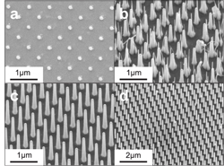 Figure 2: InP nanowire arrays created using soft nano-imprint lithography: (a) pattern of Au dots after lift-off process, prior to growth of nanowires; (b) nanowire array without suitable cleaning step with ‘grass-like’ wires appearing between intended structures; (c) and (d) nanowire array resulting from a piranha (sulfuric acid/hydrogen peroxide) cleaning step and 550°C anneal before growth.
Philips has been working with others on III-V nanowire on silicon technology for some time. For example, Bakkers was part of a group that reported a generic process for creating nearly defect-free arrays of indium phosphide (InP) and gallium phosphide (GaP) nanowires [Aurélie Pierret et al, Nanotechnology, vol21, p065305, 2010]. A patterned array of gold particles (on InP and GaP substrates, rather than silicon, in this case) formed the catalyst for the nanowire metal-organic chemical vapor deposition growth. It was found that cleaning away organic residues from the catalyst deposition and patterning was particularly important for defect-free results (Figure 2). Previous work involving Bakkers has included III-V nanowire growth on silicon.
![]() Search: III-V nanowire
Search: III-V nanowire
Visit: www.miplaza.com/index.html
The author Mike Cooke is a freelance technology journalist who has worked in the semiconductor and advanced technology sectors since 1997.
![]() ©2010 Juno Publishing and Media Solutions Ltd. All rights reserved. Semiconductor Today and the editorial material contained within it and related media is the copyright of Juno Publishing and Media Solutions Ltd. Reproduction in whole or part without permission from Juno Publishing and Media Solutions Ltd is forbidden. In most cases, permission will be granted, if the author, magazine and publisher are acknowledged.
©2010 Juno Publishing and Media Solutions Ltd. All rights reserved. Semiconductor Today and the editorial material contained within it and related media is the copyright of Juno Publishing and Media Solutions Ltd. Reproduction in whole or part without permission from Juno Publishing and Media Solutions Ltd is forbidden. In most cases, permission will be granted, if the author, magazine and publisher are acknowledged.
Disclaimer: Material published within Semiconductor Today and related media does not necessarily reflect the views of the publisher or staff. Juno Publishing and Media Solutions Ltd and its staff accept no responsibility for opinions expressed, editorial errors and damage/injury to property or persons as a result of material published.
Semiconductor Today, Juno Publishing and Media Solutions Ltd, Suite no. 133, 20 Winchcombe Street, Cheltenham, GL52 2LY, UK
Web site by No Name No Slogan ![]()