| Home | About Us | Contribute | Bookstore | Advertising | Subscribe for Free NOW! |
| News Archive | Features | Events | Recruitment | Directory |
News
18 June 2010
First CMOS-compatible III-V n-MOSFET with self-aligned contacts
Researchers based in Singapore and Taiwan have been developing self-aligned contacts for III-V metal-oxide-semiconductor field-effect transistors (MOSFETs) [Xingui Zhang et al, Symposium on VLSI Technology Digest of Technical Papers, p233, 2010]. Such devices are being developed to overcome the limitations of standard silicon complementary MOSFET (CMOS) logic integrated circuits as device sizes shrink to less than 22nm (by about 2015).
While researchers are attracted to the high mobility of III-V materials compared with silicon – giving a low on-resistance for the channel – much work has been and needs to be done to accomplish a cost-effective mass-production process for such devices with suitable characteristics.
Much progress has been made in terms of integration to silicon (enabling the use of a large, low-cost substrate), gate insulation, reducing the off-current, etc. This work has largely been carried out with micron-sized contacts. In order for III-V MOSFETs to be useful at small device scales less than 22nm, these contacts will need to be reduced by orders of magnitude in a mass-production process.
The researchers – from National University of Singapore (NUS), Taiwan Semiconductor Manufacturing Company (TSMC), Taiwan National Nano Device Laboratory, and Taiwan National Chiao-Tung University – report the first demonstration of III-V n-MOSFETs with self-aligned contacts formed using a technique compatible with CMOS processing (Figure 1).
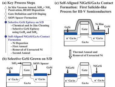
Figure 1: (a) Key process steps for first technology demonstration of Singapore/Taiwan III-V MOSFET self-aligned contact. (b) Epitaxy process for forming thin continuous GeSi layer on GaAs S/D regions, followed by (c) Ni deposition and two-step anneal process to form NiGeSi ohmic contact on GaAs.
The Singapore/Taiwan process is similar to the self-aligned silicide (salicide) contact formation step used in mainstream CMOS semiconductor production: a germanium-silicon (GeSi) layer is formed on the gallium arsenide (GaAs) source–drain regions; then nickel is deposited and rapid thermal annealed (RTA, 250°C, 30sec) so that it reacts with the GeSi; the unreacted nickel is removed in a selective process. A second anneal (RTA, 500°C, 60sec) is used to diffuse Ge and Si atoms into the GaAs contact regions, creating heavy n+-doping.
Before the contact process is performed, the gate stack of the devices was formed using hafnium-aluminum oxide insulator with a tantalum nitride gate metal. Also the source–drain regions were doped with silicon using ion implantation and an activation anneal at 850°C. The GeSi was deposited using an epitaxial process with in-situ cleaning and surface treatment that selected GaAs rather than the silicon dioxide hard mask and silicon oxynitride spacer protecting the gate. The resulting GeSi material was crystalline.
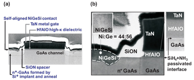
Figure 2: (a) Transmission electron micrograph (TEM) of III-V MOSFET with self-aligned contacts. (b) Zoomed-in view of NiGeSi formed on Si-implanted and annealed n+ GaAs S/D regions. A silane ammonia (SiH4+NH3) passivation was used to form high-quality gate dielectric interface on GaAs. Insets: high-resolution TEM images of NiGeSi and gate stack.
The researchers also created structures on p-GaAs substrates to measure the contact resistance of the NiGeSi material using the transmission-line method (TLM). A value of 5.7x10⁻⁴Ω/cm2 was obtained. The researchers believe that further reductions in this value are possible.
The researchers produced 33 MOSFETs with gate lengths between 0.2 and 1μm (200–1000nm). The widths of the gate were 100μm. The subthreshold swings (SSs) were in the range 200–350mV/decade (at a drain voltage of 0.1V). As the gate length reduced to 0.2μm, the threshold voltage reduced from about 1.6V to just over 1.3V.
![]() Search: III-V MOSFETs GaAs
Search: III-V MOSFETs GaAs
Visit: www.vlsisymposium.org
The author Mike Cooke is a freelance technology journalist who has worked in the semiconductor and advanced technology sectors since 1997.
![]() ©2010 Juno Publishing and Media Solutions Ltd. All rights reserved. Semiconductor Today and the editorial material contained within it and related media is the copyright of Juno Publishing and Media Solutions Ltd. Reproduction in whole or part without permission from Juno Publishing and Media Solutions Ltd is forbidden. In most cases, permission will be granted, if the author, magazine and publisher are acknowledged.
©2010 Juno Publishing and Media Solutions Ltd. All rights reserved. Semiconductor Today and the editorial material contained within it and related media is the copyright of Juno Publishing and Media Solutions Ltd. Reproduction in whole or part without permission from Juno Publishing and Media Solutions Ltd is forbidden. In most cases, permission will be granted, if the author, magazine and publisher are acknowledged.
Disclaimer: Material published within Semiconductor Today and related media does not necessarily reflect the views of the publisher or staff. Juno Publishing and Media Solutions Ltd and its staff accept no responsibility for opinions expressed, editorial errors and damage/injury to property or persons as a result of material published.
Semiconductor Today, Juno Publishing and Media Solutions Ltd, Suite no. 133, 20 Winchcombe Street, Cheltenham, GL52 2LY, UK
Web site by No Name No Slogan ![]()