| Home | About Us | Contribute | Bookstore | Advertising | Subscribe for Free NOW! |
| News Archive | Features | Events | Recruitment | Directory |
News
1 March 2010
Improving deep UV emission on aluminum nitride templates
Researchers in Japan have produced more efficient deep ultraviolet (DUV) light-emitting diodes (LEDs) emitting in the wavelength range 260–270nm. [Yusuke Sakai et al, Jpn. J. Appl. Phys., vol49, p022102, 2010]. Though comparing the performance at 30K and 300K, the researchers give a rough estimate for the internal quantum efficiency (IQE) of 33% for one arrangement.
The layers for the LED devices were grown by metal-organic chemical vapor deposition (MOCVD) on aluminum nitride (AlN) on sapphire epitaxial templates. The source gases were trimethyl-gallium TM-Ga), trimethyl-aluminum (TM-Al), ammonia (NH3), silane (SiH4, for n-type silicon doping), and cyclopentadienyl magnesium (CP2Mg, for p-type Mg doping).
The work was performed by researchers at Nagoya Institute of Technology and NGK Insulators Ltd., which produces AlN ceramic components using sintering techniques. In addition, together with Japan’s Mie University, NGK has developed a self-produced low-pressure MOCVD system to deposit layers of AlN up to a micron thick on silicon carbide and sapphire [Shibata et al, physica status solidi (c), vol0, p2023, 2003]. The growth temperature for AlN on sapphire reaches about 1000°C, which is higher than that for the subsequent epi-layers.
Two different quality AlN templates were produced. One (A) had x-ray diffraction ‘rocking curves’ (XRCs) with approximate full-width at half maximum (FWHM) values of 80arcsec and 1000arcsec for symmetrical [0002] and asymmetrical [10-12] reflections, respectively. The second (B) had narrower (and hence better-quality) values of 40arcsec and 200arcsec, respectively. Atomic force microscopy gave roughness values of less than 0.3nm for a 5μm x 5μm scan area for both templates and showed step-growth morphology.
The active light-emitting layers consisted of alternating 5nm layers of Al0.49Ga0.51N (well) and Al0.58Ga0.42N (barrier). There were five well layers, separated by four barrier layers. A thin 1nm AlN layer acted as an electron blocker to stop carrier overflow into the top p-type layers. Carrier overflow is one way of getting less efficient light emission.
 The multiple quantum wells were grown on 1μm n-type
Al0.6Ga0.4N cladding that in turn was grown on 0.5μm undoped Al0.6Ga0.4N buffer on the AlN template. The layers on the electron blocker consisted of p-type AlGaN: 25nm Al0.6Ga0.4N cladding, 25-nm p-type Al0.3Ga0.7N layer, and 200nm p-type GaN contact. An electric furnace anneal was performed at 800°C for 30 minutes in nitrogen to activate the Mg-doping. Mesa structures (0.5mm x 0.5mm) were formed and electrodes deposited in a traditional manner.
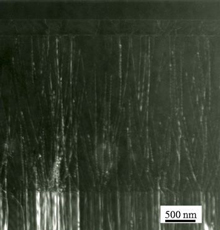
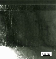 Figure 1: Cross-sectional dark-field TEM images for LED epilayers on template A (above) and template B (right).
XRC analysis was also carried out on the AlGaN epi-layers. LEDs grown on sample A had typical FWHMs of 250arcsec (symmetrical) and 800arcsec (asymmetrical). The corresponding values for sample B were 300arcsec and 400arcsec, respectively. Transmission electron microscope (TEM) studies suggested the dislocations in sample A originated from the underlying AlN material, while those in B arose from the AlN/AlGaN interface (Figure 1). The average dislocation densities were estimated at 1x10¹⁰/cm2 (A) and 4x10⁹/cm2 (B).
 Electroluminescence (EL) studies with injection currents in the range 10–50mA showed spectra centered on 265nm (A) and 267nm (B). The FWHMs were 10nm (A) and 15nm (B). There was a weak parasitic peak detected for LEDs on template A (~500nm), but not for B.
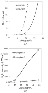
Figure 2: (a) Current-voltage (I-V, a) and light intensity-injection current characteristics (L-I, b) for DUV LEDs.
The B LEDs had a lower turn-on voltage of 10V, compared with 17V for A LEDs (Figure 2). At 50mA, the light outputs were measured at 40μW/cm2 (A) and 570μW/cm2 (B). The B LEDs were thus ten times brighter.
See related item:
Deep ultraviolet power boost at shorter wavelengths
![]() Search: DUV LEDs MOCVD AlN AlGaN
Search: DUV LEDs MOCVD AlN AlGaN
Visit: http://jjap.ipap.jp/link?JJAP/49/022102
Visit: www.ngk.co.jp/english/index.html
Visit: www3.interscience.wiley.com
![]() ©2010 Juno Publishing and Media Solutions Ltd. All rights reserved. Semiconductor Today and the editorial material contained within it and related media is the copyright of Juno Publishing and Media Solutions Ltd. Reproduction in whole or part without permission from Juno Publishing and Media Solutions Ltd is forbidden. In most cases, permission will be granted, if the author, magazine and publisher are acknowledged.
©2010 Juno Publishing and Media Solutions Ltd. All rights reserved. Semiconductor Today and the editorial material contained within it and related media is the copyright of Juno Publishing and Media Solutions Ltd. Reproduction in whole or part without permission from Juno Publishing and Media Solutions Ltd is forbidden. In most cases, permission will be granted, if the author, magazine and publisher are acknowledged.
Disclaimer: Material published within Semiconductor Today and related media does not necessarily reflect the views of the publisher or staff. Juno Publishing and Media Solutions Ltd and its staff accept no responsibility for opinions expressed, editorial errors and damage/injury to property or persons as a result of material published.
Semiconductor Today, Juno Publishing and Media Solutions Ltd, Suite no. 133, 20 Winchcombe Street, Cheltenham, GL52 2LY, UK
Web site by No Name No Slogan ![]()