| Home | About Us | Contribute | Bookstore | Advertising | Subscribe for Free NOW! |
| News Archive | Features | Events | Recruitment | Directory |
News
25 May 2010
Getting nitride HEMT gates in shape for optimum performance
The effects of varying the structure of gate electrodes in nitride semiconductor high-electron-mobility transistors (HEMTs) has been reported by researchers from the Institute of Microelectronics at the Chinese Academy of Sciences (CAS), Beijing [Wang Dongfang et al, J. Semicond., vol31, p054003, 2010].
HEMTs using aluminum gallium nitride (AlGaN) and gallium nitride (GaN) material layers are being widely developed for high-speed and high-power operation such as wireless network base-station radio signal transmission power amplification and for power switching applications such as for hybrid electric vehicles.
Although production technology outside China has enabled great progress, with devices operating at Ka-band (26.5–40GHz) and even W-band (75–110GHz) microwave frequencies with powers of up to 10.5W/mm at 40GHz, local technology is challenged in producing gate lengths below 0.25μm, meaning that the X-band (8–12GHz) is generally the limit for devices developed in the country. In addition to the engineering problem of producing shorter gate lengths, there are possible short-channel effects to concern developers, such as threshold voltage shifts, soft pinch-off, high sub-threshold currents, and thus increased off-currents.
The CAS researchers hope that, by focusing on the gate, they can squeeze better performance from their resources. In particular, they looked at T-gate structures, including Γ-structures (Figure 1). Such structures are widely used to reduce the gate resistance due to its greater cross section. Another factor is that the arm of the ‘T’ on the drain side serves as a field plate, the effect of which can be to increase the breakdown voltage of the device. Along with the positive effects of T-gates come the negative effects of parasitic capacitance that can impact high-frequency performance. Hence, as is often the case, there needs to be a complex balancing act between intended improvements and unintended deleterious consequences.
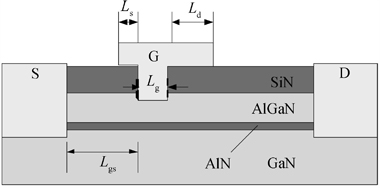
Figure 1: Schematic of AlGaN/GaN HEMT structure studied.
The nitride semiconductor wafers for the HEMTs were supplied by the Academy’s Institute of Semiconductors. The layers (Al0.25Ga0.75N/AlN/GaN) were grown using metal-organic chemical vapor deposition (MOCVD) on a sapphire substrate. The resulting wafer had a sheet resistance of 370Ω/square. The ohmic contacts were titanium-aluminum-nickel-gold (Ti/Al/Ni/Au) and the Schottky gate was Ni/Au. A silicon nitride passivation layer was deposited between the source/drain contact evaporation process and the final gate-forming process involving electron-beam lithography, dry-etch and evaporation. The actual gate length was measured at 0.35μm and the source-drain distance was 4μm. The gate width was 75μm.
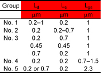 The resulting devices were separated into five comparison groups (Table). Each type was represented by no less than five examples. The groups were designed to reveal the effects of varying just one parameter. A series of DC and RF measurements were made on the devices.
Table: Five comparison groups of HEMTs.
The researchers came to a number of conclusions concerning optimized gate structures for gate lengths greater than 0.25μm.
First, reduced field-plate lengths can enhance both the current gain cutoff frequency (fT) and maximum oscillation frequency (fmax). However, a reduced field-plate also increases gate resistance, a factor that hits fmax. This resistance could be reduced by using an increased metal thickness for the gate. Reducing the T-arm on the drain side (Ld) has more effect on the frequency performance, compared with that on the source-side (Ls). Hence, one approach could be to increase Ls to reduce the gate resistance, while shortening Ld to improve frequency performance, producing what the researchers call a τ-shaped gate (Figure 2).
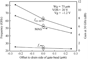 Figure 2: Frequency cut-off (fT), maximum oscillation (fmax) and maximum available gain (MAG) at 30GHz for devices with different gate-head locations (or gate shapes). The τ-shaped gate structure where
the source-side arm is longer than the drain-side arm is favored.
The other factor determining breakdown voltage is the position of the gate between the source and drain. The gate should be as close to the source electrode as possible, increasing the distance between the gate and drain, and hence reducing the electric field in that region, improving breakdown performance. It is also found that moving the gate towards the source increases the maximum drain current.
The project was supported by China’s National Science Foundation.
![]() Search: AlGaN/GaN HEMTs
Search: AlGaN/GaN HEMTs
Visit: http://dx.doi.org
The author Mike Cooke is a freelance technology journalist who has worked in the semiconductor and advanced technology sectors since 1997.
![]() ©2010 Juno Publishing and Media Solutions Ltd. All rights reserved. Semiconductor Today and the editorial material contained within it and related media is the copyright of Juno Publishing and Media Solutions Ltd. Reproduction in whole or part without permission from Juno Publishing and Media Solutions Ltd is forbidden. In most cases, permission will be granted, if the author, magazine and publisher are acknowledged.
©2010 Juno Publishing and Media Solutions Ltd. All rights reserved. Semiconductor Today and the editorial material contained within it and related media is the copyright of Juno Publishing and Media Solutions Ltd. Reproduction in whole or part without permission from Juno Publishing and Media Solutions Ltd is forbidden. In most cases, permission will be granted, if the author, magazine and publisher are acknowledged.
Disclaimer: Material published within Semiconductor Today and related media does not necessarily reflect the views of the publisher or staff. Juno Publishing and Media Solutions Ltd and its staff accept no responsibility for opinions expressed, editorial errors and damage/injury to property or persons as a result of material published.
Semiconductor Today, Juno Publishing and Media Solutions Ltd, Suite no. 133, 20 Winchcombe Street, Cheltenham, GL52 2LY, UK
Web site by No Name No Slogan ![]()