| Home | About Us | Contribute | Bookstore | Advertising | Subscribe for Free NOW! |
| News Archive | Features | Events | Recruitment | Directory |
News
17 May 2010
Prospects for full visible coverage from one nitride substrate
Building on their previous suggestion for ternary indium gallium nitride (InGaN) substrates for producing devices emitting a wide range of visible wavelength light, Tarun Sharma and Elias Towe of Carnegie Mellon University (CMU) now believe a single combination (In0.15Ga0.85N) could cover the needs for red, green and blue radiation [T. K. Sharma and E. Towe, Appl. Phys. Lett., vol96, p191105, 2010]. By concentrating efforts on one combination, it is to be hoped that the development of useful devices could be accelerated.
The researchers believe this approach could fill the ‘green gap’ for producing laser diodes (LDs) for projector systems. Presently, the red and blue emissions are usually covered by using gallium arsenide and gallium nitride substrates, respectively. Unfortunately, the green light in such devices need to come from a less compact, less efficient arrangement, involving frequency doubling of infrared LD emissions, for example.
Another beneficiary from filling the gap could be better low-cost high color rendering index (CRI) white light emitting diode (LED) arrangements to replace inefficient incandescent lighting. Present low-cost ‘white’ LEDs often use a blue-emitting diode to power a yellow phosphor. This creates a ‘white’ CRI of around 70, rather than the 100 of blackbody emitters such as incandescent and sun light. By filling in the green, a balanced, direct RGB emission should become available that would allow better control of CRI and color temperature. As the technology develops, costs would fall.
In principle, nitride semiconductors should be able to cover the wavelength range from ~2500nm infrared (indium nitride) down through the visible to ~200nm ultraviolet (aluminum nitride). However, the comfort zone for nitride semiconductor technology at present is inside the rather narrower range 500nm-300nm (blue-green to ultraviolet).
One of the main difficulties in exploiting the full potential of nitride semiconductors is growing high quality indium gallium nitride (InGaN) alloy crystal layers on gallium nitride substrates caused by strain arising from the difference in lattice constants between the materials. Large strains generate performance-killing defects and dislocations.
Recently a number of techniques have been proposed and demonstrated to improve material quality, such as using GaN substrates of different crystal orientation, allowing laser wavelengths as long as 530nm in pulsed-mode and 520nm in continuous operation. However, the improvements in performance from such strategies over devices grown on the more mature c-plane GaN seem slight (c-plane devices have reached out to 515nm).
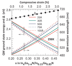 Figure 1: Ground state energy of compressively strained InGaN QWs grown on In0.15Ga0.85N substrate plotted as a function of composition for different values of QW thicknesses. The corresponding QW emission wavelength is shown on the right axis. The energy gap between the first and second conduction band at the Γ-point (k = 0) for InxGa1−xN layers is also plotted (Δ).
Sharma and Towe have carried out a series quantum mechanical ‘envelope function’ calculations of the energy levels for InGaN quantum wells (QWs) grown on an In0.15Ga0.85N ‘application oriented nitride substrate’ (AONS). The calculation took account of various strain effects such as modification of the band structure and changes in hole effective mass. With higher indium content in the well, leading to compressively strained InGaN, the researchers hope that green (520-570nm) and even red (630-740nm) emission could be achieved, particularly adding in an expected red-shift of up to 30nm for such devices arising from internal polarization electric fields (Figure 1).
The possibility of blue (440-490nm) requires consideration of the complexities of the three valence bands under tensile strain. The researchers believe that QW devices based on tensile strain layers could lead to lower threshold currents in LDs, with the resulting laser light being transverse magnetic polarized. However, producing useful LEDs could be hindered by the emission direction tending to be in the planes, rather than in the direction of layer growth.
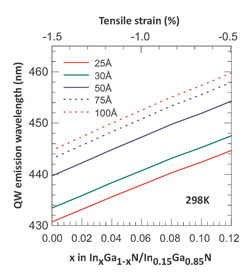 Figure 2: Emission wavelength of tensile strain InGaN QWs grown on In0.15Ga0.85N substrate as a function of composition for different values of QW thicknesses.
The researchers modeled QWs in lattice-matched AlInGaN barriers with an energy difference of about 300meV (Figure 2). The emissions came in the range 430nm-460nm with various well thicknesses and compositions. Even shorter wavelengths (up to 50nm) should be possible using AlGaN wells, giving violet coverage.
Sharma and Towe also suggest that the use of InGaN substrates could avoid the resonant Auger effect suggested last year as the source of efficiency droop in InGaN LEDs. The resonant Auger mechanism couples electron-hole energies (conduction to valence band) to promoting a second electron from the lowest conduction band to a higher band, rather than producing a photon. This effect would be strongest where the difference between the higher and lowest conduction band (Δ) is close to the QW ground state energy. The AONS QW calculation suggests that the effect should only be significant up to around 1% compressive strain (Figure 1).
These calculations are only suggestive since commercial high-quality InGaN substrates do not as yet exist. However, alloy substrates do exist in other material systems such as for arsenide and antimonide semiconductors (InGaAs and InGaSb). In addition, a wide range of techniques are available for growing InGaN material. “There seems to be no fundamental reason preventing the development of InGaN AONS,” Sharma and Towe write. The researchers also suggest that there may be opportunities for ultraviolet detectors and emitters based on InAlN or AlGaN substrates.
See related item:
Application-oriented quantum theory for infrared nitride lasers?
![]() Search: InGaN substrates Green gap Laser diodes
Search: InGaN substrates Green gap Laser diodes
Visit: http://link.aip.org
The author Mike Cooke is a freelance technology journalist who has worked in the semiconductor and advanced technology sectors since 1997.
![]() ©2010 Juno Publishing and Media Solutions Ltd. All rights reserved. Semiconductor Today and the editorial material contained within it and related media is the copyright of Juno Publishing and Media Solutions Ltd. Reproduction in whole or part without permission from Juno Publishing and Media Solutions Ltd is forbidden. In most cases, permission will be granted, if the author, magazine and publisher are acknowledged.
©2010 Juno Publishing and Media Solutions Ltd. All rights reserved. Semiconductor Today and the editorial material contained within it and related media is the copyright of Juno Publishing and Media Solutions Ltd. Reproduction in whole or part without permission from Juno Publishing and Media Solutions Ltd is forbidden. In most cases, permission will be granted, if the author, magazine and publisher are acknowledged.
Disclaimer: Material published within Semiconductor Today and related media does not necessarily reflect the views of the publisher or staff. Juno Publishing and Media Solutions Ltd and its staff accept no responsibility for opinions expressed, editorial errors and damage/injury to property or persons as a result of material published.
Semiconductor Today, Juno Publishing and Media Solutions Ltd, Suite no. 133, 20 Winchcombe Street, Cheltenham, GL52 2LY, UK
Web site by No Name No Slogan ![]()