| Home | About Us | Contribute | Bookstore | Advertising | Subscribe for Free NOW! |
| News Archive | Features | Events | Recruitment | Directory |
News
26 May 2010
UV APD improved by m-plane free-standing GaN substrate
The Center for Quantum Devices (CQD) at Northwestern University has turned to the capabilities of m-plane gallium nitride as an ultraviolet photodetector [Z. Vashaei et al, Appl. Phys. Lett., p96, p201908, 2010].
Lower dark currents and higher gains were achieved compared with previous attempts to produce GaN-based avalanche photodiodes (APDs) by using m-plane oriented free-standing gallium nitride substrates that are now being offered by commercial suppliers, particularly with a view to improved light-emission applications such as for green laser diodes. The m-plane crystal orientation is also attractive for APD applications since the ionization coefficients in such devices is expected to be larger than that for more conventional c-plane GaN.
The researchers are working towards replacing bulky fragile glass photo-multiplier tubes (PMTs) with III-nitride based ultraviolet APDs. The operating voltage of PMTs is typically 1kV. The internal gain of 106 for these devices leads to very low dark currents (noise) compared with systems using traditional semiconductors such as silicon or silicon carbide. Si and SiC semiconductor devices also need filtering to cut out visible/solar wavelengths.
Aluminum gallium nitride (AlGaN) semiconductor APDs would have frequency cut-offs determined by their energy bandgaps roughly in the range 3.4eV (GaN) up to 6.2eV (AlN), corresponding to wavelengths between 365nm and 200nm, respectively. Such devices would therefore be naturally blind to visible spectrum/solar wavelengths (greater than 380nm).
Previous attempts to produce nitride APDs have used sapphire or SiC substrates. Lattice mismatches in such systems lead to high dislocation densities (~109/cm2), which increases leakage currents and limits the possibility for avalanche gain. Avalanche gain occurs when carriers under a reverse bias gain enough energy to generate further electron–hole pairs, creating a cascade (Figure 1).
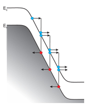 Figure 1: Avalanche breakdown mechanism.
Metal-organic chemical vapor deposition (MOCVD) using tri-methyl gallium (TMG) and ammonia (NH3) was employed to create the device layers. Silane (SiH4) and Bis(cyclopentadienyl)magnesium (DCpMg) were used to give n-type and p-type doping, respectively. After some disappointing attempts at growing GaN layers on the m-plane GaN, it was found that a desorption step carried out at high temperature was needed to remove contaminants such as oxygen or silicon from the substrate surface. Further work was carried out to optimize the MOCVD growth conditions for maximum crystal quality for both undoped and doped layers.
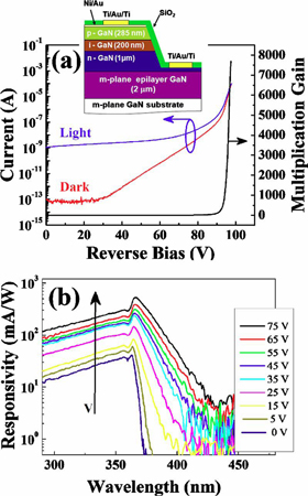 Figure 2: (a) Current-voltage and multiplication gain-voltage characteristics for 225μm2 area m-plane GaN APDs. Inset: cross-sectional diagram of device structure. (b) Responsivity measurements with increasing reverse bias voltage (V).
The APD structures consisted of a 2μm undoped template layer, followed by 1μm of n-GaN, 200nm of i-GaN, and 285nm p-GaN, forming a p-i-n diode (Figure 2). The ohmic n-type contact consisted of nickel-gold, and the p-contact titanium-gold-titanium. The devices were created in the form of 225μm2 circular mesas. A silicon dioxide passivation layer was also deposited to prevent surface leakage and breakdown effects.
The dark current of the resulting device was below the measurement limit of CQD’s equipment (a Hewlett-Packard HP4155A semiconductor parameter analyzer) up to 30V reverse bias. At 50V reverse bias, the dark current was 8.11pA (3.6x10⁻⁶A/cm2 density). Above 80V reverse bias, the dark current increased rapidly. For comparison, one reported value for a GaN APD on c-plane sapphire had a dark current density of 6.4x10⁻³A/cm2. The significant reduction in leakage current for the new device is attributed to “development of high-quality homoepitaxial growth on low-defect-density FS-GaN substrates”.
Increasing the reverse bias increases the spectral response near the 364nm band edge (Figure 2b). The band-edge response at 0V is 41.5mA/W (external quantum efficiency 14.2%) and at 70V 523.0mA/W (EQE 177%). The increase in reverse bias red-shifts the band edge slightly due to the change in optical absorption in a semiconductor with applied electric field (the Franz-Keldysh effect).
The onset of avalanche multiplication was determined to be at 25V (unity gain). A sharp increase in gain was observed after 84V reverse bias with a maximum gain of 8000 found at 97V.
The researchers hope that further improvements/ optimizations in design and fabrication processing could enhance the gain significantly for front-illumination.
![]() Search: UV APD Free-standing GaN substrate
Search: UV APD Free-standing GaN substrate
Visit: http://link.aip.org
The author Mike Cooke is a freelance technology journalist who has worked in the semiconductor and advanced technology sectors since 1997.
![]() ©2010 Juno Publishing and Media Solutions Ltd. All rights reserved. Semiconductor Today and the editorial material contained within it and related media is the copyright of Juno Publishing and Media Solutions Ltd. Reproduction in whole or part without permission from Juno Publishing and Media Solutions Ltd is forbidden. In most cases, permission will be granted, if the author, magazine and publisher are acknowledged.
©2010 Juno Publishing and Media Solutions Ltd. All rights reserved. Semiconductor Today and the editorial material contained within it and related media is the copyright of Juno Publishing and Media Solutions Ltd. Reproduction in whole or part without permission from Juno Publishing and Media Solutions Ltd is forbidden. In most cases, permission will be granted, if the author, magazine and publisher are acknowledged.
Disclaimer: Material published within Semiconductor Today and related media does not necessarily reflect the views of the publisher or staff. Juno Publishing and Media Solutions Ltd and its staff accept no responsibility for opinions expressed, editorial errors and damage/injury to property or persons as a result of material published.
Semiconductor Today, Juno Publishing and Media Solutions Ltd, Suite no. 133, 20 Winchcombe Street, Cheltenham, GL52 2LY, UK
Web site by No Name No Slogan ![]()