| Home | About Us | Contribute | Bookstore | Advertising | Subscribe for Free NOW! |
| News Archive | Features | Events | Recruitment | Directory |
News
19 May 2010
Multi-story production of optoelectronics from GaAs release
Researchers based in the USA and South Korea have developed techniques for producing a number of device levels that are then released and transferred to a separate substrate for further processing [Jongseung Yoon et al, Nature, vol465, p329, 2010]. The main research was carried out by University of Illinois Urbana-Champaign, with some contributions from personnel associated with Hanyang University in Seoul and Semprius, a company based in North Carolina.
The researchers grew a variety of aluminum gallium arsenide (AlGaAs) layers on GaAs substrates using metal-organic chemical vapor deposition (MOCVD). Silicon and zinc were used for n- and p-type doping, respectively.
Patterned vertical etching with a citric acid-hydrogen peroxide solution created an array of rectangular columns. Separate device levels were separated by high Al content Al0.95Ga0.05As that has a much higher etch rate in hydrofluoric (HF) acid compared with material of low Al content (Figure 1). A patterned photoresist layer was used to hold the devices in place while they were etched away from the underlying wafer.
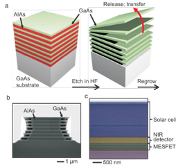 Figure 1: Schematic of multilayer GaAs/AlAs stack and the release of membranes through selective etching of AlAs layers (a). Also shown are SEM cross-sections after partial etch of AlAs layers (b) and a colored image of a heterogeneous device (c).
The devices were then transferred to suitable substrates for further processing. Separately, Semprius is developing micro-transfer printing technology to create concentrator photovoltaic (CPV) products. The North Carolina-based company also offers licenses for applications of the printing technique to non-CPV applications such as flat-panel displays, flexible electronics, large-area sensors, and RF devices.
Three device types were produced and tested using the techniques described in the Nature paper: metal-semiconductor field-effect transistors (MESFETs), near-infrared (NIR) detectors, and photovoltaic (PV) cells. In one case, all three device-type layers were produced on a single substrate (Figure 1). In other cases, the three devices types were produced on separate wafers with multiple layers – 7 or 40 bilayers of (n-GaAs/Al0.95Ga0.05As for the MESFETs, 4 repeats of n-GaAs/GaAs/Al0.95Ga0.05As for the NIR detectors, and 3 repeats of n-GaAs/n-Al0.4Ga0.6As/n-GaAs/p-GaAs/p-Al0.3Ga0.7As/p-GaAs/Al0.95Ga0.05As for the solar cells.
The MESFET device membranes were transferred to glass substrates coated with a thin layer of polyimide. The devices were pattern etched to form the channel regions of width 130μm and length 25μm. The ohmic source and drain contacts were made of palladium-germanium-gold (Pd/Ge/Au) and a 3μm Schottky gate of titanium-gold (Ti/Au). Using the top five layers of a 7-repeat wafer, the researchers found the performance variations between the layers to be ‘random with magnitudes comparable to device-to-device variations observed in any given single layer’. The frequency performance of the devices demonstrated unity current gain (fT) and unity power gain (fmax) frequencies of ~2 and ~6GHz, respectively. Separate devices on the glass substrate could be interconnected to form NAND and NOR gates.
For the NIR detectors, a silicon substrate was chosen since this material is often used for infrared imagers. The detector consisted of a Schottky metal contact, n-GaAs and an ohmic contact, with the same metal combinations as for the MESFET. The structure provides a NIR photodiode and a Schottky diode to block reverse bias current, preventing crosstalk in a passive matrix readout set-up. On-off ratios of ~200 were found, a figure sufficient for passive operation. Elements derived from all four layers showed comparable performance. The elements were assembled into a 16x16 array. The yield for functioning pixels was ~96%. Assembly into interconnected arrays resulted in pixel yields of 70%, an indication that the present limitation is breaks in wiring.
PV membranes constituted the third demonstration of the technology. Here the substrate was 50μm thick flexible polyethylene terephthalate (PET) sheets (Figure 2). The n-type ohmic contact consisted of Pd/Ge/Au and the p-type of the sequence platinum-titanium-platinum-gold (Pt/Ti/Pt/Au). In contrast to the previous cases, the performance of the resulting PV cell did show some fall-off in short-circuit current performance with the source level of the membrane. Secondary ion mass spectrometry suggests that diffusion of Zn in the p-type layers is to blame for the shift in performance. The researchers propose that an alternative dopant with a lower diffusion coefficient, such as carbon, could solve this problem.
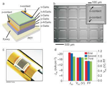
Figure 2: Schematic (a) of GaAs single-junction solar cell on a PET substrate coated with a photodefinable epoxy. Optical image (b) of arrays of such devices formed on the source wafer. Inset, magnified view of top (n-type) and bottom (p-type) contacts. Photograph (c) of a solar module consisting of a 10x10 array of 500x500μm GaAs solar cells on a PET substrate. Graph (d) shows measured short-circuit current density (Jsc), fill factor (FF) and open circuit voltage (Voc) under simulated AM1.5D (air mass 1.5 direct) illumination (1000W/m2) at room temperature with a single-layer anti-reflection coating (ARC, Si3N4) of first, second and third layer devices.
With a double layer anti-reflective coating (ARC), the devices can reach 20.5% efficiency, which compares very favorably with some of the best reported devices designed for ultrahigh concentration photovoltaic operation (20.6%). The cells can be connected in various ways – series, parallel or a combination – to deliver a variety of voltage and current performance.
The researchers also see opportunities for these techniques in other material systems such as those grown on gallium nitride or indium phosphide substrates. This could open the way to new forms of light emitting diodes, lasers and sensors.
![]() Search: AlGaAs GaAs substrates MOCVD
Search: AlGaAs GaAs substrates MOCVD
Visit: http://dx.doi.org/10.1038/nature09054
Visit: http://www.semprius.com
The author Mike Cooke is a freelance technology journalist who has worked in the semiconductor and advanced technology sectors since 1997.
![]() ©2010 Juno Publishing and Media Solutions Ltd. All rights reserved. Semiconductor Today and the editorial material contained within it and related media is the copyright of Juno Publishing and Media Solutions Ltd. Reproduction in whole or part without permission from Juno Publishing and Media Solutions Ltd is forbidden. In most cases, permission will be granted, if the author, magazine and publisher are acknowledged.
©2010 Juno Publishing and Media Solutions Ltd. All rights reserved. Semiconductor Today and the editorial material contained within it and related media is the copyright of Juno Publishing and Media Solutions Ltd. Reproduction in whole or part without permission from Juno Publishing and Media Solutions Ltd is forbidden. In most cases, permission will be granted, if the author, magazine and publisher are acknowledged.
Disclaimer: Material published within Semiconductor Today and related media does not necessarily reflect the views of the publisher or staff. Juno Publishing and Media Solutions Ltd and its staff accept no responsibility for opinions expressed, editorial errors and damage/injury to property or persons as a result of material published.
Semiconductor Today, Juno Publishing and Media Solutions Ltd, Suite no. 133, 20 Winchcombe Street, Cheltenham, GL52 2LY, UK
Web site by No Name No Slogan ![]()