- News
29 November 2010
Altatech launches system for inspecting wafer edges and controlling multi-layer overlap
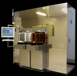
 At this week’s SEMICON Japan 2010 trade show (1–3 December), Altatech Semiconductor S.A. of Montbonnot, near Grenoble, France is launching its high-throughput AltaSight EyeEdge inspection system, which can detect, identify and generate images of defects as small as 2 microns along the edges of 300mm wafers, including compound semiconductor, silicon, silicon-on-insulator (SOI), quartz and transparent substrates. Applications include inspecting bare or patterned wafers, through-silicon vias (TSVs) used in 3D semiconductor integration, and thin-film layer overlap at the extreme edges (the crown or apex) of wafers.
Available as either a stand-alone tool or as a modular, fully retrofitable enhancement on Altatech’s 300mm AltaSight platform, the EyeEdge system maximizes device yield and profitability by finding and accurately classifying defects that other inspection schemes (including laser-scanning systems) cannot, the firm claims. In addition, throughput of 100 300mm wafers per hour enables EyeEdge to achieve higher productivity than other inspection systems on the market, it adds.
“We developed EyeEdge based on close communications with our strategic partners in the semiconductor market, whose requirements for critical edge inspection and cost-of-ownership performance are incorporated into this new product,” says president Jean-Luc Delcarri.
Altatech says that it has installed two beta-site systems at customers’ R&D laboratories, where the equipment is being qualified for use in volume production.
Designed for a wide range of users — from wafer suppliers to integrated device manufacturers (IDMs) and foundries to product development laboratories — EyeEdge is a fully automated defect-classification system that comes standard with three high-speed optical sensors for single-pass inspection. Using Altatech’s proprietary DeepSight technology, these sensors collect sufficient data to define the size, shape and location of defects anywhere within 1.5mm of a wafer’s edge. EyeEdge then generates a three-dimensional image of each surface anomaly for easy classification.
“The ability to detect minute shifts in optical signals is critically important at the edges of wafers, where thin-film overlapping and delamination issues complicate the inspection process,” says Delcarri. “More expensive laser-scan inspection systems cannot discriminate between real defects and false, irrelevant signals. Faced with wafer-to-wafer variations, laser systems are not adaptive enough to continually changing noise/signal ratios,” he adds. “Furthermore, relying on scattered light information limits the ability to accurately classify defects in today's production environments.”
EyeEdge is designed to accommodate an optional fourth optical sensor to analyze a programmable crown area on a wafer’s front-side edge. While maintaining the system’s processing accuracy and high throughput, the additional sensor enables EyeEdge to measure layer-overlapping control, providing what is claimed to be a unique high-speed, low-cost solution to control insulating, barrier and seed layers, copper electroplating and chemical mechanical planarization (CMP), photoresist edge-bead removal (EBR) and edge-cleaning effectiveness.
EyeEdge is a stand-alone system, but can be added as a module onto the AltaSight platform to create a holistic system that can inspect a wafer’s front-side, back-side and edge simultaneously using a combination of reflectivity, topographical, dark-field and DeepSight technologies.
“We have fuelled our innovation with continued customer interaction and partnership and a large breadth of technologies in our IP portfolio,” says Delcarri. “We have quickly converted them into productive products and brought them to the market,” he adds. “The demand is out there. As everyone is striving for improved performance, our engineering team, sales and support services are being expanded worldwide to solve our customers’ challenges.”
