| Home | About Us | Contribute | Bookstore | Advertising | Subscribe for Free NOW! |
| News Archive | Features | Events | Recruitment | Directory |
News
9 November 2010
Fine-patterned SiGe halves power consumption of optical waveguide switch
At this week’s 23rd Annual Meeting of the IEEE Photonics Society (PHO 2010) in Denver, CO, USA (7–11 November), Japan’s Fujitsu Laboratories Ltd is reporting that it has been able to halve the power consumption of an optical waveguide switch based on silicon photonics through what is claimed to be the first use of fine-patterned silicon germanium (SiGe) for this application, rather than conventional silicon (Si). The firm says that the achievement should enable high-speed optical switches capable of operating across a wide range of wavelengths, while featuring the world’s lowest power requirements.
Fujitsu says that its new technology will help to contain power consumption while supporting large-volume network traffic, enabling high-end services linking multiple cloud networks and ultra-high-definition video-conferencing, among other applications.
With the spread of data-intensive network services such as cloud computing and ultra-high-definition video distribution, the volume of data being transmitted over networks looks set to rise continuously. Accordingly, the amount of electricity consumed by networking equipment in 2025 is predicted to be 13 times the 2006 figure if no energy-saving measures are taken (according to the Japan Ministry of Economy, Trade and Industry’s ‘Green IT Initiative’ report, December 2007), leading to concerns about potentially serious energy shortages in the future.
Conventionally, switching between optical network paths requires that signals be converted from light to electricity and back again to light in order to be processed, requiring considerable power. An optical switch that processes optical signals as they are — without the need for conversion to electricity — would therefore greatly reduce its power requirements. This issue has spurred ongoing R&D for next-generation networks.
A optical waveguide switch is a design that arrays multiple optical switching elements in series, between an optical-signal input point and output point. By combining the operations of each optical switching element, a desired optical signal path can be created (see Figure 1).
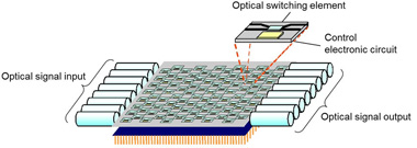
Figure 1: Optical waveguide switch using silicon photonics technology.
An optical waveguide switch employing silicon photonics uses well-established silicon fabrication technology, allowing inexpensive mass production. Furthermore, optical switch devices based on nanometer-scale waveguides and control electronic circuits can be aligned in large numbers on the same substrate, so large-scale optical switches can be fabricated compactly, measuring just a few centimeters squared.
Large-scale optical-waveguide switches operate multiple optical switching elements simultaneously. However, the heat that this generates can degrade device performance, necessitating the lowest possible power consumption for each optical switching element.
With optical switching elements, the application of an electrical current to the refractive-index modulator causes electrons to accumulate in fine waveguides, which modulates the refractive index and switches the output port (Figure 2). With conventional optical switching elements made using fine-patterned silicon, the electron-accumulation efficiency in fine silicon waveguides is low, necessitating more current to achieve sufficient electron-accumulation, increasing power consumption.

Figure 2: Top view of optical switching element.
Fujitsu has therefore developed what it reckons is the first optical switching element that uses fine-patterned SiGe in the refractive-index modulator (Figure 3). Forming fine-patterned SiGe (which has a narrower energy bandgap than silicon) on top of silicon allows more efficient electron accumulation, and hence less power is required for switching.
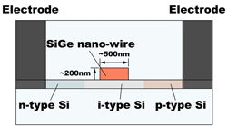 Figure 3: Cross section of refractive-index modulator.
Prototype optical switch devices developed by Fujitsu operated on 1.5mW of power (about half the power required for conventional fine-patterned silicon optical switching elements), representing what is claimed to be the lowest power requirement in the world for an optical switching element capable of high-speed operation across a wide range of wavelengths.
Fujitsu says that it aims to proceed with the development of large-scale integration as well as the integration technology for control electronic circuits, in order to realize large-scale optical switches enabling next-generation networks.
Part of Fujitsu’s research was undertaken as part of the ‘Vertically Integrated Center for Technologies of Optical Routing toward Ideal Energy Savings’ (VICTORIES) project, under the program ‘The Formation of Innovation Center for Fusion of Advanced Technologies’ sponsored by the Special Coordination Funds for Promoting Science and Technology, of Japan’s Ministry of Education, Culture, Sports, Science and Technology (MEXT).
![]() Search: Fujitsu Laboratories Optical waveguide switch Silicon photonics SiGe
Search: Fujitsu Laboratories Optical waveguide switch Silicon photonics SiGe
Visit: http://jp.fujitsu.com/labs/en
For more: Latest issue of Semiconductor Today
![]() ©2010 Juno Publishing and Media Solutions Ltd. All rights reserved. Semiconductor Today and the editorial material contained within it and related media is the copyright of Juno Publishing and Media Solutions Ltd. Reproduction in whole or part without permission from Juno Publishing and Media Solutions Ltd is forbidden. In most cases, permission will be granted, if the author, magazine and publisher are acknowledged.
©2010 Juno Publishing and Media Solutions Ltd. All rights reserved. Semiconductor Today and the editorial material contained within it and related media is the copyright of Juno Publishing and Media Solutions Ltd. Reproduction in whole or part without permission from Juno Publishing and Media Solutions Ltd is forbidden. In most cases, permission will be granted, if the author, magazine and publisher are acknowledged.
Disclaimer: Material published within Semiconductor Today and related media does not necessarily reflect the views of the publisher or staff. Juno Publishing and Media Solutions Ltd and its staff accept no responsibility for opinions expressed, editorial errors and damage/injury to property or persons as a result of material published.
Semiconductor Today, Juno Publishing and Media Solutions Ltd, Suite no. 133, 20 Winchcombe Street, Cheltenham, GL52 2LY, UK
Web site by No Name No Slogan ![]()