- News
19 November 2010
Controlling self-catalysed GaAs nanowires on silicon
Researchers in Denmark and Israel have developed methods to create higher-quality gallium arsenide (GaAs) nanowires (NWs) on silicon without using a gold catalyst [Peter Krogstrup et al, Nano Lett., vol10, p4475, 2010]. In particular the nanowires had significantly reduced numbers of twinning plane defects and a high aspect ratio (55–60nm in diameter, 8–9μm in length). The work was carried out at University of Copenhagen’s Niels Bohr Institute and Israel’s Weizmann Institute of Science.
Gallium arsenide NWs have many potential optoelectronic applications such as collecting solar energy, light detection and light emission (laser and non-laser). Sunflake A/S (a Danish company developing III-V nano-structured solar cells) is cited in the paper as being among the supporters of the research.
As a III-V compound semiconductor, GaAs can create higher-efficiency solar cells compared with silicon, but it is a much more expensive material. Producing high-quality III-V materials on inexpensive silicon wafers could lower costs for such high-efficiency devices. Apart from being made of a low-cost bulk material, silicon wafers are also available with large diameters of 300mm (with 450mm being developed by some companies), promising economies of scale.
Gold is commonly used as a catalyst to create GaAs nanowires on silicon. However, using gold as a catalyst for growth tends to create unintended deep energy levels in the nanowire material. These deep levels can act as recombination centers that degrade the electronic and photonic performance of these materials. For example, in solar cells such recombination would impact conversion efficiency.
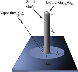 The Niels Bohr–Weizmann nanowires are grown on 2-inch diameter undoped (111) silicon wafers using solid-source molecular beam epitaxy (MBE). The growth occurs through a vapor–liquid–solid mechanism (Figure 1).
Figure 1: Schematic of Ga-assisted growth model, illustrating different effective collection areas for adatoms contributing to the NW growth.
The native oxide layer on the silicon is thought to affect the initiation of gold-free nanowire growth. ‘Native oxide’ refers to the silicon dioxide layer that naturally forms when silicon is exposed to air. In fact, previous work has used specially prepared oxide layers. The NW growth is thought to be initiated by defects or sub-nanometer pinholes in this oxide layer.
The Niels Bohr–Weizmann work suggests that gallium droplets are formed on the surface of the wafer which, on reaching a critical size, become supersaturated and hence begin NW growth, ‘most likely through oxide dissolution at the droplet/substrate interface’. The size of the critical droplet controls the diameter of the subsequent NW to within 10%.
The size of the droplets is mainly controlled by temperature and the partial pressures of the source material. The window for GaAs NW growth temperatures was found to be 590–670°C, below which only GaAs chunks rather than wires were deposited and above which no GaAs growth occurred at all.
Further control of the wire diameter could be achieved by thinning the native oxide layer. Fully oxidized native layers resulted in 40nm NW diameters, but approximately halving the oxide thickness using a thermal oxide desorption at 1100°C and controlled subsequent oxidation at 100°C gave NWs with 18–20nm diameter.
The researchers made considerable experimental and theoretical efforts to understand and control the growth of their NWs to achieve pure cubic zinc blende (ZB) GaAs crystal structure, eliminating as far as possible the presence of hexagonal wurtzite (WZ) layers. In particular, the team wanted to avoid ‘twin planes’, where a WZ layer can be regarded as nestling between mirror-reflected ZB structures. Another important aspect is to avoid non-vertical wires that can grow in poorly controlled conditions.
The researchers make three proposals for achieving such control to give crystal purity (no twinning planes) and for obtaining vertical non-tapered wires:
- Reduce the gallium flux to the point there is no nucleation of NWs, and then increase it until a sufficient density of wires is achieved.
- Maximize the temperature until GaAs sticking to the wafer is almost zero.
- Remove the few remaining twinning planes, and reduce the arsenic flux slightly.
The last suggestion is described as ‘surprising’. Its effect is to increase the wire diameter slightly; it also reduces their length. As can be seen, these proposals put the system close to the edge of the respective growth windows in terms of temperature and source material fluxes.
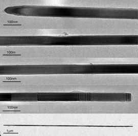 Using these principles, the researchers obtained NWs (Figure 2) that were 55–60nm in diameter and 8–9μm in length. The growth time was 45 minutes. These wires were free of twinning planes except near the root of the wire. The researchers suggest that these twinning planes could be removed by reducing the gallium flux and/or increasing the temperature. However, they comment: ‘This is a difficult task since these parameters are already close to the threshold value of initiating NW growth, however it should in principle be possible.’
Figure 2. Long and thin NWs with ZB structure achieved after optimizing Ga flux, temperature, and As flux, grown with the final parameters, fGa = 9.25×10⁻⁸Torr, fAs2 = 1.0×10⁻⁵Torr, T = 660°C.
The researchers believe that such a demonstration of pure ZB NWs has not been reported before for a gold-free process.
One advantage for working near the threshold for NW growth is a lower density of wires, which avoids interactions between the wires and could provide compatibility with set-ups where the wires need coating.
The author Mike Cooke is a freelance technology journalist who has worked in the semiconductor and advanced technology sectors since 1997.