| Home | About Us | Contribute | Bookstore | Advertising | Subscribe for Free NOW! |
| News Archive | Features | Events | Recruitment | Directory |
News
5 October 2010
Zinc oxide nano-wire on gallium nitride lights up
Researchers Babak Nikoobakht and Andrew Herzing at the US National Institute of Standards and Technology (NIST) have developed a zinc oxide (ZnO) nanowire on gallium nitride (GaN) light-emitting diode (LED) [ACS Nano, published online 15 September 2010].
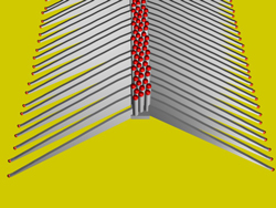 Figure 1: Single row of nanowires (cylinders with red tops) with fin-shaped nanowalls extending outward.
The nanowires are grown at 900°C using solid-vapor-liquid-solid deposition in a tube furnace with a gold catalyst previously deposited and patterned on the GaN substrate. The GaN substrate was a commercial product (from TDI) with p-type magnesium doping (Mg concentration ~ 5x10¹⁷/cm3). The zinc source comes from a ZnO-graphite mixture placed on a silicon substrate. Ultra-dry nitrogen is used as a carrier gas.
Unlike many ZnO nanowire growth methods, NIST creates ZnO nanowires in the plane of the GaN substrate, rather than perpendicular/vertical forests of nanowires. As the NIST ZnO wire grows horizontally it pushes the gold nanoparticle along the GaN surface. The direction of growth depends on the crystal structure of the substrate and also on the direction of flow of the carrier gas — the growth tends to be into the wind. Further control of the growth direction can be achieved by laying down lines of gold to block growth in particular directions.
In previous work, NIST researchers used an 8nm nanoparticle catalyst. In the new research, they increased the nanoparticle size to 20nm for some of their experiments. This resulted in wires that grew secondary shark-like ‘dorsal fins’ or ‘nano-walls’. The height of the nano-wall gradually decreases as one goes toward the leading edge where the nano-particle is. This suggests that the further growth is due to a slower self-catalytic process on the wire created by the nano-particle.
The ZnO material in these structures is n-type conducting (i.e. the moveable charge carriers, ‘electrons’, are negatively charged, with density ~ 1018/cm3). The individual heterojunctions measure about 10μm long and 80nm wide.
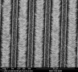 Figure 2: Transmission electron micrograph (TEM) shows four rows of nanowires and their corresponding nanowalls. Distance across the micrograph is about the diameter of a human hair.
Various characterizations were performed – such as selected area diffraction (SAD) pattern and x-ray energy-dispersive spectroscopic (XEDS) imaging – that suggested that the junction between the ZnO and GaN crystal structures was abrupt.
When charge crossed the p-n GaN–ZnO junction, light was emitted, creating what Nikoobakht and Herzing call nano-LEDs. The current was injected with titanium-gold electrodes for the n-ZnO contact and nickel-gold for the p-GaN contact.
Under forward bias the emission was around the violet 390nm (3.18eV) wavelength (32nm full-width half-maximum), which is related by the researchers to the ZnO exciton (electron–hole bound state with a binding energy of ~60meV). The strong exciton emission would suggest that most of the forward-bias recombination occurred in the ZnO crystal structure, with holes being injected from the underlying p-GaN.
Light was also emitted under reverse bias — around an orange wavelength of 640nm (1.95eV). The intensity of the radiation reduced in smaller devices, with better rectifying behavior and higher breakdown voltage (9V rather than 4V). The researchers suggest that this emission could result from a transition between an intrinsic shallow state to a deep state such as those associated with oxygen vacancies. The researchers say that the source of the reverse bias emission is ‘still under study’.
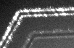 Figure 3: TEM image of nano-LEDs emitting light.
Nikoobakht and Herzing hope to improve the nano-LEDs in future by using a better geometry and material design. The researchers hope to apply the devices in a number of contexts, giving light sources and detectors for photonic devices or lab-on-a-chip microsystem platforms.
These devices could be powered by nano-generators. For example, zinc oxide is commonly used in prototype nano-generator systems that depend on vibration, since it has a powerful piezoelectric effect (strain-dependent polarization electric field). Meanwhile, nitride semiconductors are being developed by some as solar cell materials.
The researchers suggest that similar techniques could be used to grow ZnO nano-structures on other nitrides such as indium gallium nitride or aluminum gallium nitride.
![]() Search: NIST ZnO nanowire GaN substrate LEDs
Search: NIST ZnO nanowire GaN substrate LEDs
Visit: http://pubs.acs.org/doi/abs/10.1021/nn1019972
For more: Latest issue of Semiconductor Today
The author Mike Cooke is a freelance technology journalist who has worked in the semiconductor and advanced technology sectors since 1997.
![]() ©2010 Juno Publishing and Media Solutions Ltd. All rights reserved. Semiconductor Today and the editorial material contained within it and related media is the copyright of Juno Publishing and Media Solutions Ltd. Reproduction in whole or part without permission from Juno Publishing and Media Solutions Ltd is forbidden. In most cases, permission will be granted, if the author, magazine and publisher are acknowledged.
©2010 Juno Publishing and Media Solutions Ltd. All rights reserved. Semiconductor Today and the editorial material contained within it and related media is the copyright of Juno Publishing and Media Solutions Ltd. Reproduction in whole or part without permission from Juno Publishing and Media Solutions Ltd is forbidden. In most cases, permission will be granted, if the author, magazine and publisher are acknowledged.
Disclaimer: Material published within Semiconductor Today and related media does not necessarily reflect the views of the publisher or staff. Juno Publishing and Media Solutions Ltd and its staff accept no responsibility for opinions expressed, editorial errors and damage/injury to property or persons as a result of material published.
Semiconductor Today, Juno Publishing and Media Solutions Ltd, Suite no. 133, 20 Winchcombe Street, Cheltenham, GL52 2LY, UK
Web site by No Name No Slogan ![]()