| Home | About Us | Contribute | Bookstore | Advertising | Subscribe for Free NOW! |
| News Archive | Features | Events | Recruitment | Directory |
News
27 September 2010
Al-Ga co-doped ZnO conducting layer boosts nitride tunnel junction LED
Korean researchers from Lumimicro Co Ltd, Kyungpook National University, Korea Photonics Technology Institute, and Pukyong National University have been developing zinc oxide (ZnO) as a transparent conducting layer for use with nitride light-emitting diodes (LEDs) with the aim of increasing photon extraction [Tae Hoon Kim et al, Jpn. J. Appl. Phys., vol49, p091002, 2010].
Transparent conducting layers (TCLs) are desired for many applications such as LEDs and photovoltaic solar cells to increase the amount of light either leaving or entering the device. In nitride LEDs, thin layers of nickel (Ni) and gold (Au) can be used to create TCLs, but the transparency is rather low at 60–75%. In other applications, such as thin-film solar cell production, indium tin oxide (ITO) is a popular choice. However, indium is a very expensive material to use.
The desired qualities for a TCL are high transparency and low resistivity: these qualities can be achieved with ZnO films with aluminum, gallium or indium doping. However, ZnO films generally have an n-type character. Unfortunately, there is no process available to produce p-type ZnO layers with any measure of stability.
For use in LEDs, one needs the TCL to make ohmic contact with the p-type gallium nitride (GaN) that is normally the top layer of nitride LEDs. Unfortunately, with n-ZnO on p-GaN one expects a Schottky contact behavior that increases the forward voltage (indicating energy loss/high contact resistance) and also deterioration of performance with temperature.
A further quality needed for the use of doped ZnO as a TCL is a low deposition temperature, since one does not want to disturb the previous hard work that has gone into depositing high-quality nitride layers.
It is possible to make ohmic contact between n-ZnO and p-GaN using a thin metal layer, but this requires an undesirable high-temperature anneal step. The Korean researchers preferred to use a silicon-doped (n-type) tunnel junction as an intermediary between the p-GaN and the ZnO TCL.
The Al-Ga co-doped ZnO (AGZO) TCL was applied to commercial 2-inch LED epiwafers from Korean supplier Epivalley. The layer structure consisted of undoped GaN (3μm), heavy silicon-doped (n++) GaN (2μm), n-GaN (0.5μm), a GaN/InGaN multi-quantum well (MQW) active region, magnesium-doped (p) GaN (0.2μm), and a 10nm tunnel junction layer. The tunnel junction consisted of a three-period GaN/In0.17Ga0.83N structure. This was topped off with a 300nm AGZO TCL, deposited using RF sputtering.
The LED chips were fabricated using lithography and wet etching. Comparison devices using nickel-gold TCLs were also produced. Conventional packaging using epoxy encapsulation was employed.
Before creating the LEDs, a number of experiments were carried out on sapphire to optimize the AGZO deposition process with the aim of achieving low resistivity and high transparency. Using RF sputtering with an argon partial pressure of 1.5mTorr, it is possible to obtain AGZO films with 96.3% transparency at 460nm wavelengths (blue) and 6.8x10⁴Ω-cm resistivity (carrier concentration 4.9x10²⁰/cm3).
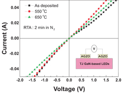 Figure 1: Current–voltage characteristics of TJ GaN-based LEDs with AGZO transparent conducting layer as a function of annealing temperature. Inset: measurement configuration.
The AGZO TCLs on the LEDs were characterized with various levels of annealing (Figure 1). Without the anneal, the AGZO-TJ contact was close to ohmic, with a small difference between the work functions: 4.6eV for the AGZO and 4.2eV for the TJ layer. Slight improvement in the ohmic behavior was seen for annealing at 550°C, but Schottky-type behavior occurred at the higher anneal temperature of 650°C. The researchers comment that Ga-doped indium oxide (In2O3) and indium tin oxide (solid solution of In2O3 and SnO2) TCLs show similar trends with annealing temperature.
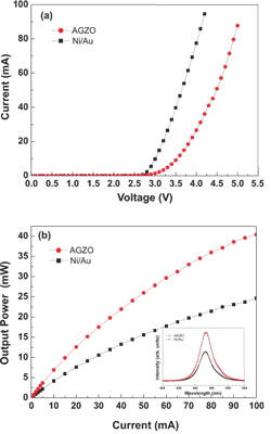 Figure 2: Comparisons of AGZO (300nm) and Ni/Au (5/5nm) TCLs: (a) current–voltage, (b) light output power vs current, and (inset) emission spectra.
The LEDs produced using an AGZO contact had an increased forward voltage (meaning higher contact resistance) than the Ni/Au comparison devices (Figure 2). For example, at a driving current of 20mA the forward voltage was 3.84V, which is 0.67V higher than for the Ni/Au LED. The specific contact resistance between the AGZO and TJ layers is estimated to be 10-2-10-3Ω-cm2. In general, AGZO on GaN has a contact resistance that is one or two orders of magnitude higher than that of Ni/Au on GaN.
Although the higher resistance of the AGZO contact suggests energy losses, the light output power, with a peak at a wavelength of 453nm, is higher than for the comparison Ni/Au contact. At 20mA, the AGZO LED had an output power of 12.6mW and the Ni/Au LED 7.6mW. These give external quantum efficiencies of 23.0% and 13.9% respectively (23.0% = 1.65x13.9%). This improvement for the AGZO device is due to the higher transparency of the contact layer: 96.3% rather than 70% for the Ni-Au layer at 460nm.
In addition to LEDs, the researchers see AGZO thin films as being promising materials for transparent conducting electrodes in applications such as touch panels, solar cells, and organic LEDs (OLEDs). However, leading nitride LEDs without a tunnel junction have achieved external quantum efficiencies of about 60%, so obviously commercial use is going to need more development.
Visit: http://jjap.ipap.jp/link?JJAP/49/091002
Visit: www.lumimicro.com
Visit: www.epivalley.com
For more on ZnO: Latest issue of Semiconductor Today
The author Mike Cooke is a freelance technology journalist who has worked in the semiconductor and advanced technology sectors since 1997.
![]() ©2010 Juno Publishing and Media Solutions Ltd. All rights reserved. Semiconductor Today and the editorial material contained within it and related media is the copyright of Juno Publishing and Media Solutions Ltd. Reproduction in whole or part without permission from Juno Publishing and Media Solutions Ltd is forbidden. In most cases, permission will be granted, if the author, magazine and publisher are acknowledged.
©2010 Juno Publishing and Media Solutions Ltd. All rights reserved. Semiconductor Today and the editorial material contained within it and related media is the copyright of Juno Publishing and Media Solutions Ltd. Reproduction in whole or part without permission from Juno Publishing and Media Solutions Ltd is forbidden. In most cases, permission will be granted, if the author, magazine and publisher are acknowledged.
Disclaimer: Material published within Semiconductor Today and related media does not necessarily reflect the views of the publisher or staff. Juno Publishing and Media Solutions Ltd and its staff accept no responsibility for opinions expressed, editorial errors and damage/injury to property or persons as a result of material published.
Semiconductor Today, Juno Publishing and Media Solutions Ltd, Suite no. 133, 20 Winchcombe Street, Cheltenham, GL52 2LY, UK
Web site by No Name No Slogan ![]()